

| Distributor | Stock | Pricing | MOQ | PKG | Lead Time | Date Code | On Order Quantity | On Order Delivery | |
|---|---|---|---|---|---|---|---|---|---|
|
3,600 pcs
|
3600 pcs | On Request | 1 | On Request | On Request | On Request | On Request | On Request |
| Category | |
| Manufacturer Name | |
| Clock Frequency | |
| Current | |
| Function | |
| Input Capacitance | |
| Lead Style | |
| Max Propagation Delay @ V, Max CL | |
| Mounting Type | |
| Number of Bits per Element | |
| Number of Elements | |
| Operating Temperature | |
| Output Type | |
| Supplier Device Package | |
| Supplier Package | |
| Trigger Type | |
| Type | |
| Voltage |
The CD4027BCN from On Semiconductor is a dual J-K master/slave flip-flop integrated circuit. It is constructed with complementary MOS (CMOS) technology, offering a wide supply voltage range from 3V to 15V. Each flip-flop includes independent J, K, set, reset, and clock inputs, along with buffered Q and Q outputs. The device is edge-sensitive to the clock input, changing state on the positive-going transition of clock pulses. Set or reset operations are independent of the clock and are achieved by a high level on the respective input.
This flip-flop IC operates at a typical clock frequency of 15.5 MHz and has a maximum propagation delay of 130ns at 15V and 50pF. It features a typical input capacitance of 5 pF and a quiescent device current of 4 µA. The operating temperature range is -55°C to 125°C (TA).
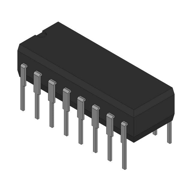
The CD4027BCN is designed for Through Hole mounting and comes in a 16-PDIP package. All inputs are protected against static discharge damage by diode clamps to VDD and VSS. This component is suitable for various digital logic applications requiring reliable flip-flop functionality.
| Qty | Low | High |
|---|---|---|
| 1+ | $1.23 | $1.23 |
Estimated market price range - modelled values for guidance only, not live distributor offers.
3V to 15V.
16-DIP (0.300", 7.62mm) with through-hole mounting.
-55°C to 125°C.
15.5 MHz (12 MHz at 10V supply).
130 ns at 15V, 50 pF load.
Positive edge.
Complementary (Q and Q̅).