

| Distributor | Stock | Pricing | MOQ | PKG | Lead Time | Date Code | On Order Quantity | On Order Delivery | |
|---|---|---|---|---|---|---|---|---|---|
|
1,160 pcs
|
1160 pcs | On Request | 1 | On Request | On Request | On Request | On Request | On Request |
| Category | |
| Manufacturer Name | |
| AEC Qualified | |
| Automotive Grade | |
| Current | |
| Drain to Source Voltage (Vdss) | |
| FET Type | |
| Input Capacitance (Ciss) (Max) @ Vds | |
| Mounting Type | |
| Operating Temperature Range | |
| Power Dissipation | |
| Rds On (Max) @ Id, Vgs | |
| Supplier Device Package | |
| Tape & Reel | |
| Technology | |
| Vgs(th) (Max) @ Id |
The BSS84LT1 is a single P-Channel MOSFET manufactured by On Semiconductor (onsemi). It features a maximum drain-to-source voltage (Vdss) of -50 V and a continuous drain current of -130 mA at 25°C ambient temperature. The device is built with MOSFET (Metal Oxide) technology and is designed for surface mount assembly.
Key electrical characteristics include a typical drain-to-source on-resistance (Rds(on)) of 4.7 Ohms at VGS = -5 V and ID = -100 mA, with a maximum of 10 Ohms. The gate threshold voltage (Vgs(th)) ranges from -0.9 V to -2.0 V at ID = -250 µA. The device can dissipate up to 225 mW at 25°C ambient and operates over a junction temperature range of -55°C to 150°C.
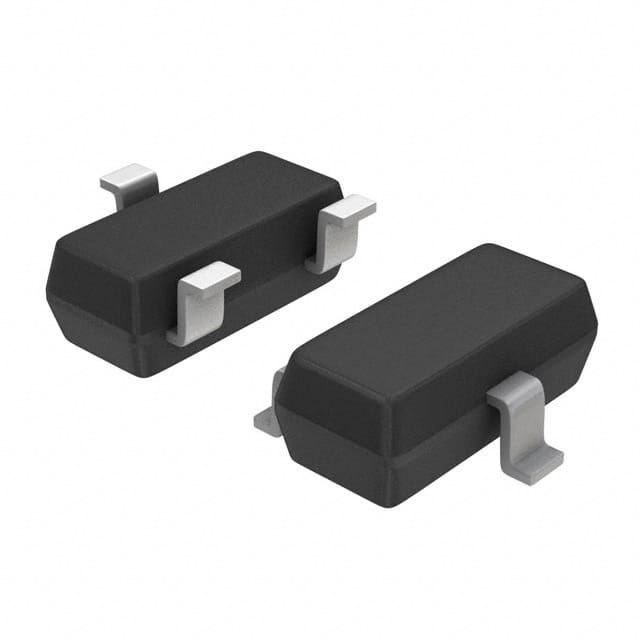
The BSS84LT1 is supplied in the industry-standard SOT-23 surface mount package (Case 318), which saves board space. It is Pb-Free and RoHS compliant. This part is suitable for low-power load switching and general-purpose applications where a P-Channel MOSFET is required.
The maximum drain-to-source voltage (Vdss) is -50 V.
The continuous drain current is -130 mA at TA = 25°C.
The BSS84LT1 is available in a SOT-23 surface mount package (Case 318).
The operating and storage temperature range is -55°C to 150°C.
Yes, the BSS84LT1 is RoHS3 compliant and Pb-Free.
The typical drain-to-source on-resistance is 4.7 Ohms at VGS = -5 V and ID = -100 mA.
The gate threshold voltage (Vgs(th)) ranges from -0.9 V to -2.0 V at VDS = VGS and ID = -250 µA.