

| Distributor | Stock | Pricing | MOQ | PKG | Lead Time | Date Code | On Order Quantity | On Order Delivery | |
|---|---|---|---|---|---|---|---|---|---|
|
2,026,020 pcs
|
2026020 pcs | On Request | 1 | On Request | On Request | 1928+ | On Request | 2026-06-03 08:15:10 | |
|
2,395 pcs
|
2395 pcs | On Request | 1 | On Request | On Request | On Request | On Request | On Request |
| Category | |
| Manufacturer Name | |
| AEC Qualified | |
| Automotive Grade | |
| Configuration | |
| Current | |
| Drain to Source Voltage (Vdss) | |
| FET Feature | |
| Halogen Free | |
| Input Capacitance (Ciss) (Max) @ Vds | |
| Mounting Type | |
| Operating Temperature | |
| Power | |
| Rds On (Max) @ Id, Vgs | |
| Storage Temperature | |
| Supplier Device Package | |
| Tape & Reel | |
| Technology | |
| Termination Finish | |
| Vgs(th) (Max) @ Id | |
| Weight |
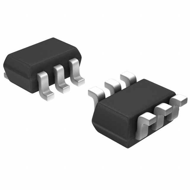
The BSS8402DWQ-7 is a complementary pair enhancement mode MOSFET from Diodes Incorporated, designed for general purpose interfacing switch and power management functions. It integrates both N-channel and P-channel MOSFETs in a single SOT-363 package.
Key electrical specifications include a drain-source voltage of 60V for Q1 (N-channel) and -50V for Q2 (P-channel), with maximum continuous drain currents of 115mA and -130mA respectively. The on-resistance is 13.5Ω at VGS=10V for Q1 and 10Ω at VGS=-5V for Q2. The device features logic level gate drive, low input capacitance of 50pF, and a gate threshold voltage of 2.5V.
The MOSFET is surface mountable in the SOT-363 package, which is also known as 6-TSSOP or SC-88. It is rated for operation from -55°C to 150°C junction temperature and has a maximum power dissipation of 200mW. The device is RoHS3 compliant, lead-free, and halogen-free.
The BSS8402DWQ variant is specifically qualified for automotive applications, being AEC-Q101 qualified, PPAP capable, and manufactured in IATF 16949 certified facilities. It is suitable for applications requiring specific change control.
| Qty | Low | High |
|---|---|---|
| 1+ | $0.73 | $0.73 |
| 10+ | $0.45 | $0.45 |
| 100+ | $0.29 | $0.29 |
| 500+ | $0.22 | $0.22 |
| 1,000+ | $0.20 | $0.20 |
| 3,000+ | $0.16 | $0.16 |
Estimated market price range - modelled values for guidance only, not live distributor offers.
The N-channel MOSFET (Q1) has a drain-source voltage of 60V, and the P-channel MOSFET (Q2) has a drain-source voltage of -50V.
The BSS8402DWQ-7 is available in a SOT-363 surface mount package, also known as 6-TSSOP or SC-88.
The operating temperature range is -55°C to 150°C (junction temperature).
Yes, the BSS8402DWQ-7 is RoHS3 compliant, lead-free, and halogen-free.
The N-channel MOSFET has a maximum on-resistance of 13.5Ω at VGS=10V, and the P-channel MOSFET has a maximum on-resistance of 10Ω at VGS=-5V.