

| Distributor | Stock | Pricing | MOQ | PKG | Lead Time | Date Code | On Order Quantity | On Order Delivery | |
|---|---|---|---|---|---|---|---|---|---|
|
174,000 pcs
|
174000 pcs | On Request | 1 | On Request | On Request | 18+ | On Request | On Request | |
|
28,020 pcs
|
28020 pcs | On Request | 1 | On Request | On Request | On Request | On Request | On Request | |
|
1,200 pcs
|
1200 pcs | On Request | 1 | On Request | On Request | On Request | On Request | On Request | |
|
997 pcs
|
997 pcs | On Request | 1 | On Request | On Request | On Request | On Request | On Request |
| Category | |
| Manufacturer Name | |
| Configuration | |
| Current | |
| Drain to Source Voltage (Vdss) | |
| FET Feature | |
| Halogen Free | |
| Input Capacitance (Ciss) (Max) @ Vds | |
| Mounting Type | |
| Operating Temperature | |
| Power | |
| Rds On (Max) @ Id, Vgs | |
| SVHC Present | |
| Supplier Device Package | |
| Tape & Reel | |
| Technology | |
| Vgs(th) (Max) @ Id | |
| Weight |
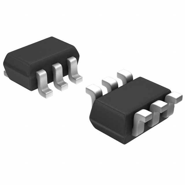
The BSS8402DW-7-F is a complementary pair enhancement mode MOSFET from Diodes Incorporated, combining an N-Channel and P-Channel device in a single SOT-363 surface mount package. The N-Channel transistor is rated for a maximum drain-to-source voltage of 60V and a continuous drain current of 115mA, while the P-Channel transistor is rated for -50V and -130mA. The device features a logic level gate, with a maximum gate threshold voltage of 2.5V at 250µA, and a maximum on-resistance of 7.5Ohm at 50mA and 5V.
This MOSFET is designed for low on-resistance and fast switching, making it suitable for general purpose interfacing switches, power management functions, and analog switch applications. The complementary N/P configuration allows for simplified circuit design in applications requiring both device types. The device is housed in a SOT-363 (SC-70-6) package, which is a small surface mount package suitable for compact PCB layouts.
The BSS8402DW-7-F is totally lead-free and fully RoHS compliant, and is halogen and antimony free. The device is rated for operation over a junction temperature range of -55°C to 150°C, with a maximum power dissipation of 200mW. The package is rated UL 94V-0, and the device is moisture sensitivity level 1 per J-STD-020. The device is available in tape and reel packaging with 3,000 units per reel.
This complementary MOSFET pair is suitable for power management and general purpose switching applications where low on-resistance and low gate threshold voltage are required. The SOT-363 package is compact and suitable for space-constrained designs. The device is also available in automotive grade variants (BSS8402DWQ-7 and BSS8402DWQ-13) that are AEC-Q101 qualified and PPAP capable.
| Qty | Low | High |
|---|---|---|
| 1+ | $0.71 | $0.71 |
| 10+ | $0.47 | $0.47 |
| 100+ | $0.30 | $0.30 |
| 500+ | $0.20 | $0.20 |
| 3,000+ | $0.20 | $0.20 |
Estimated market price range - modelled values for guidance only, not live distributor offers.
The N-Channel MOSFET (Q1) has a maximum drain-to-source voltage of 60V, and the P-Channel MOSFET (Q2) has a maximum drain-to-source voltage of -50V.
The N-Channel MOSFET (Q1) has a maximum drain current of 115mA, and the P-Channel MOSFET (Q2) has a maximum drain current of -130mA.
The maximum on-resistance is 7.5 ohms at a drain current of 50mA and gate-source voltage of 5V.
The operating junction temperature range is -55°C to 150°C.
The field is available in a 6-TSSOP, SC-88, SOT-363 package, with the supplier device package being SOT-363.
Yes, the field is RoHS3 compliant, fully compliant with EU Directive 2002/95/EC (RoHS), 2011/65/EU (RoHS 2) and 2015/863/EU (RoHS 3).
The maximum power dissipation is 200mW.