

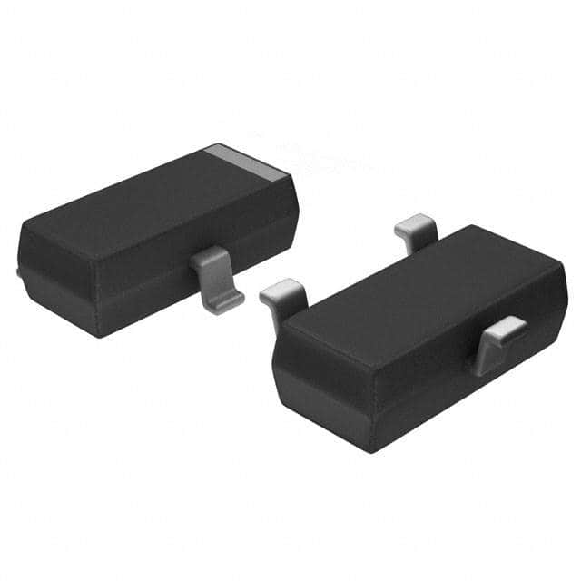
| Distributor | Stock | Pricing | MOQ | PKG | Lead Time | Date Code | On Order Quantity | On Order Delivery | |
|---|---|---|---|---|---|---|---|---|---|
|
2,250 pcs
|
2250 pcs | On Request | 1 | On Request | On Request | On Request | On Request | On Request |
| Category | |
| Manufacturer Name | |
| AEC Qualified | |
| Automotive Grade | |
| Current | |
| Drain to Source Voltage (Vdss) | |
| Drive Voltage (Max Rds On, Min Rds On) | |
| FET Type | |
| Gate Charge (Qg) (Max) @ Vgs | |
| Halogen Free | |
| Input Capacitance (Ciss) (Max) @ Vds | |
| Mounting Type | |
| Operating Temperature | |
| Power Dissipation (Max) | |
| Rds On (Max) @ Id, Vgs | |
| SVHC Present | |
| Storage Temperature | |
| Supplier Device Package | |
| Tape & Reel | |
| Technology | |
| Vgs (Max) | |
| Vgs(th) (Max) @ Id |
The Infineon BSS670S2L is an N-channel enhancement mode MOSFET from the OptiMOS buck converter series. It is designed for low-voltage switching applications requiring a drain-source voltage of 55V and a continuous drain current of 540mA at 25°C. The device features a maximum on-resistance of 650mΩ at VGS=10V and 825mΩ at VGS=4.5V, making it suitable for logic-level gate drive.
This MOSFET is avalanche rated with a single-pulse avalanche energy of 8.1mJ. It offers fast switching with typical turn-on delay of 9ns, rise time of 25ns, turn-off delay of 21ns, and fall time of 24ns. The gate charge is typically 1.7nC, enabling efficient switching at moderate frequencies.
The device is qualified according to AEC Q101 and is halogen-free per IEC61249-2-21. It is packaged in a PG-SOT23 surface-mount package and is supplied in tape and reel (3000 pcs/reel). The operating junction temperature range is -55°C to +150°C.
| Qty | Low | High |
|---|---|---|
| 1+ | $0.34 | $0.34 |
| 10+ | $0.21 | $0.21 |
| 100+ | $0.13 | $0.13 |
| 500+ | $0.10 | $0.10 |
| 1,000+ | $0.09 | $0.09 |
| 3,000+ | $0.07 | $0.07 |
| 6,000+ | $0.07 | $0.07 |
| 9,000+ | $0.05 | $0.05 |
| 24,000+ | $0.05 | $0.05 |
Estimated market price range - modelled values for guidance only, not live distributor offers.
The maximum drain-source voltage (VDS) is 55V.
The continuous drain current is 540mA at TA=25°C and 430mA at TA=70°C.
The device is available in PG-SOT23 surface-mount package (also known as TO-236-3, SC-59, SOT-23-3).
The operating junction temperature range is -55°C to +150°C.
RoHS status is listed as 'RoHS3 Compliant' but is unverified. The datasheet confirms halogen-free compliance per IEC61249-2-21.
The typical total gate charge (Qg) is 1.7nC at VDD=40V, ID=0.54A, VGS=0 to 10V.
The maximum on-resistance is 650mΩ at VGS=10V, ID=270mA.