

| Distributor | Stock | Pricing | MOQ | PKG | Lead Time | Date Code | On Order Quantity | On Order Delivery | |
|---|---|---|---|---|---|---|---|---|---|
|
12,000 pcs
|
12000 pcs | On Request | 1 | On Request | On Request | On Request | On Request | On Request |
| Category | |
| Manufacturer Name | |
| AEC Qualified | |
| Automotive Grade | |
| FET Feature | |
| FET Type | |
| Gate Charge | |
| Industrial Grade | |
| Input Capacitance | |
| Medical Grade | |
| Military Grade | |
| Mounting Type | |
| Operating Temperature | |
| Power Dissipation | |
| Supplier Device Package | |
| Technology |
The Infineon BSS139H6906XTSA1 is an N-Channel MOSFET designed for various electronic applications. It features a high drain-to-source voltage (Vdss) of 250V and a continuous drain current (Id) of 100mA at 25°C.
Key electrical characteristics include a maximum on-resistance (Rds On) of 14 Ohms at 100mA and 10V, an input capacitance (Ciss) of 76pF at 25V, and a gate charge (Qg) of 3.5nC at 5V. The device operates with a gate threshold voltage (Vgs(th)) of 1V at 56µA and can withstand a gate-to-source voltage (Vgs) of up to ±20V.
This MOSFET has a maximum power dissipation of 360mW (Ta) and operates within a temperature range of -55°C to 150°C. It is a depletion mode FET, utilizing MOSFET (Metal Oxide) technology.
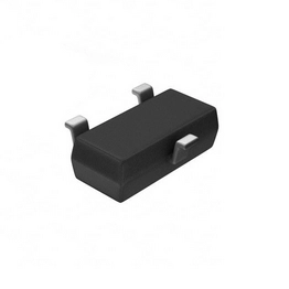
The BSS139H6906XTSA1 is supplied in a compact SOT-23-3 surface-mount package, making it suitable for space-constrained designs. Its supplier device package is identified as PG-SOT23-3-5.
| Qty | Low | High |
|---|---|---|
| 1+ | $0.99 | $0.99 |
Estimated market price range - modelled values for guidance only, not live distributor offers.
The maximum drain-to-source voltage (Vdss) for the BSS139H6906XTSA1 is 250V.
The continuous drain current (Id) at 25°C is 100mA.
The maximum on-resistance (Rds On) is 14 Ohms when tested at 100mA drain current and 10V gate-source voltage.
The operating temperature range is from -55°C to 150°C.
The BSS139H6906XTSA1 is supplied in a SOT-23-3 surface-mount package.