

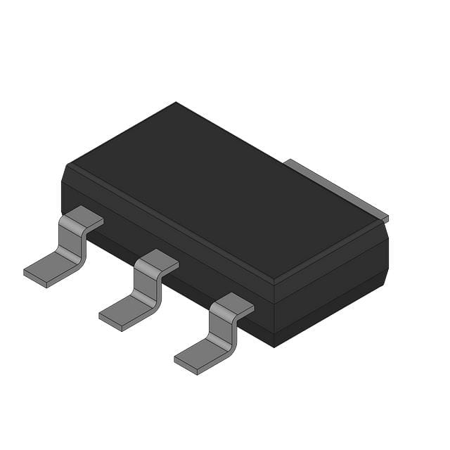
| Distributor | Stock | Pricing | MOQ | PKG | Lead Time | Date Code | On Order Quantity | On Order Delivery | |
|---|---|---|---|---|---|---|---|---|---|
|
1,000 pcs
|
1000 pcs | On Request | 1 | On Request | On Request | On Request | On Request | On Request |
| Category | |
| Manufacturer Name | |
| Current | |
| Drain to Source Voltage (Vdss) | |
| Drive Voltage (Max Rds On, Min Rds On) | |
| FET Type | |
| Gate Charge (Qg) (Max) @ Vgs | |
| Input Capacitance (Ciss) (Max) @ Vds | |
| Mounting Type | |
| Operating Temperature | |
| Power Dissipation (Max) | |
| Rds On (Max) @ Id, Vgs | |
| Supplier Device Package | |
| Tape & Reel | |
| Technology | |
| Vgs (Max) | |
| Vgs(th) (Max) @ Id |
The BSP295L6327 is a small-signal N-channel enhancement-mode MOSFET manufactured by Infineon Technologies. It is designed for low-power switching and signal amplification applications where moderate voltage and current levels are required.
Key electrical specifications include a maximum drain-source voltage (Vdss) of 60V and a continuous drain current of 1.8A at ambient temperature. The device features a low on-resistance of 300mOhm (maximum) at a drain current of 1.8A and gate-source voltage of 10V, enabling efficient conduction. The gate charge is 17nC (maximum at 10V) and input capacitance is 368pF (maximum at 25V), indicating moderate switching performance. The gate threshold voltage is 1.8V (maximum at 400µA), and the recommended drive voltages are 4.5V and 10V. Maximum gate-source voltage is ±20V.
Thermally, the MOSFET can dissipate up to 1.8W at ambient temperature and operates over a junction temperature range of -55°C to 150°C. No package or mounting information is available in the provided data. This component is suitable for general-purpose low-power switching and load control applications.
60V
-55°C to 150°C (TJ)
Maximum 300mOhm at 1.8A, 10V
Maximum 17nC at 10V
Maximum 1.8V at 400µA
±20V