

| Distributor | Stock | Pricing | MOQ | PKG | Lead Time | Date Code | On Order Quantity | On Order Delivery | |
|---|---|---|---|---|---|---|---|---|---|
|
4,000 pcs
|
4000 pcs | On Request | 1 | 6 | On Request | 13+ | On Request | On Request |
| Category | |
| Manufacturer Name | |
| AEC Qualified | |
| Automotive Grade | |
| Avalanche Energy | |
| Configuration | |
| Current | |
| Diode Continuous Forward Current | |
| Diode Forward Voltage | |
| Diode Pulse Current | |
| Drain to Source Voltage (Vdss) | |
| ESD Rating | |
| FET Feature | |
| Fall Time | |
| Gate Charge (Qg) (Max) @ Vgs | |
| Gate Threshold Voltage | |
| Gate plateau voltage | |
| Gate-Source Voltage | |
| Gate-to-Drain Charge | |
| Gate-to-Source Charge | |
| Halogen Free | |
| Input Capacitance | |
| Input Capacitance (Ciss) (Max) @ Vds | |
| Mounting Type | |
| Operating Temperature | |
| Output Capacitance | |
| Power | |
| Pulsed Drain Current | |
| Qualification | |
| Rds On (Max) @ Id, Vgs | |
| Reverse Diode dv/dt | |
| Reverse Recovery Charge | |
| Reverse Recovery Time | |
| Reverse Transfer Capacitance | |
| Rise Time | |
| Soldering Temperature | |
| Standard Package Qty | |
| Storage Temperature | |
| Supplier Device Package | |
| Tape & Reel | |
| Technology | |
| Thermal Resistance Junction-to-Ambient | |
| Total Gate Charge | |
| Transconductance | |
| Turn-Off Delay Time | |
| Turn-On Delay Time | |
| Vgs(th) (Max) @ Id | |
| continuous_drain_current (Maximum @ TA=70 °C) | |
| drain_source_on_resistance (Typical/Maximum @ VGS=2.5 V, ID=0.7 A) | |
| drain_source_on_resistance (Typical/Maximum @ VGS=4.5 V, ID=1.5 A) |
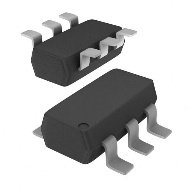
The Infineon BSL214NL6327HTSA1 is a dual N-channel enhancement mode MOSFET designed for small-signal switching applications. It features a drain-source breakdown voltage of 20V and a continuous drain current of 1.5A at 25°C (1.2A at 70°C). The device is rated for a maximum power dissipation of 500mW at 25°C and operates over a junction temperature range of -55°C to 150°C.
This MOSFET incorporates logic level gate drive with a gate threshold voltage of 0.7V min, 0.95V typ, and 1.2V max. The on-resistance is 140 mOhm max at VGS=4.5V and 250 mOhm max at VGS=2.5V. It offers fast switching with typical turn-on delay of 4.1 ns and turn-off delay of 6.8 ns. The total gate charge is 0.8 nC typical.
The BSL214NL6327HTSA1 is qualified to AEC Q101, making it suitable for automotive environments. It is RoHS3 compliant, 100% lead-free, and halogen free. The device is packaged in a PG-TSOP6 (TSOP-6) surface mount package and is supplied in tape and reel with 3000 pieces per reel.
20 V.
1.5 A at TA=25°C, 1.2 A at TA=70°C.
PG-TSOP6 (TSOP-6) surface mount package.
-55°C to 150°C (junction).
Yes, RoHS3 compliant.
Yes, qualified according to AEC Q101.
0.7 V min, 0.95 V typ, 1.2 V max at ID=3.7 µA.