

| Distributor | Stock | Pricing | MOQ | PKG | Lead Time | Date Code | On Order Quantity | On Order Delivery | |
|---|---|---|---|---|---|---|---|---|---|
|
34,000 pcs
|
34000 pcs | On Request | 1 | On Request | On Request | 08+PB | On Request | On Request | |
|
11,140 pcs
|
11140 pcs | On Request | 1 | On Request | On Request | 0828+ | On Request | On Request |
| Category | |
| Manufacturer Name | |
| Current | |
| Drain to Source Voltage (Vdss) | |
| Drive Voltage (Max Rds On, Min Rds On) | |
| FET Type | |
| Gate Charge (Qg) (Max) @ Vgs | |
| Input Capacitance (Ciss) (Max) @ Vds | |
| Mounting Type | |
| Operating Temperature | |
| Power Dissipation (Max) | |
| Rds On (Max) @ Id, Vgs | |
| Supplier Device Package | |
| Tape & Reel | |
| Technology | |
| Termination Style | |
| Vgs (Max) | |
| Vgs(th) (Max) @ Id |
The BSL211SPL6327 is a P-Channel enhancement mode MOSFET from Infineon Technologies, part of the OptiMOS-P small-signal transistor family. It is designed for low-voltage power management applications, offering a drain-source breakdown voltage of -20V and a continuous drain current of -4.7A at 25°C ambient temperature. The device features a maximum drain-source on-resistance of 67mΩ at VGS=-4.5V and ID=-4.7A, with a typical value of 54mΩ, enabling efficient power switching.
This MOSFET is rated as Super Logic Level, meaning it can be driven at gate-source voltages as low as 2.5V, making it suitable for battery-powered and low-voltage logic circuits. The gate threshold voltage ranges from -0.6V to -1.2V, allowing for straightforward interface with microcontrollers and other low-voltage drivers. The device also supports a maximum gate-source voltage of ±12V and offers a total gate charge of 12.4nC maximum, contributing to fast switching performance.
The BSL211SPL6327 is avalanche rated and has a reverse diode dv/dt rating of -6kV/µs, providing robustness in inductive load switching applications. It operates over a junction temperature range of -55°C to 150°C and dissipates up to 2W at 25°C ambient. The device is qualified to AEC Q101, making it suitable for automotive applications.
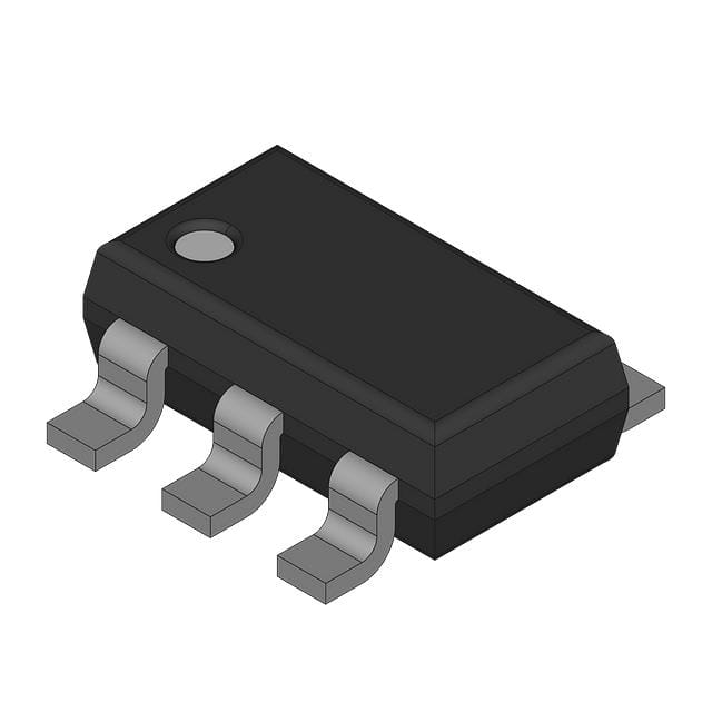
Packaged in the compact P-TSOP6-6 (TSOT-23-6) surface mount package, the BSL211SPL6327 is supplied in tape and reel format with 3000 pieces per reel. It features Pb-free lead plating and is RoHS compliant, supporting environmentally conscious manufacturing requirements.
The drain-source breakdown voltage is -20V (minimum).
The continuous drain current is -4.7A at TA=25°C and -3.8A at TA=70°C.
The drain-source on-resistance is 54mΩ typical and 67mΩ maximum at VGS=-4.5V and ID=-4.7A. At VGS=-2.5V and ID=-3.7A, it is 94mΩ typical and 110mΩ maximum.
The operating junction temperature range is -55°C to 150°C.
Yes, the device is RoHS compliant with Pb-free lead plating, as stated in the datasheet.
The device comes in a P-TSOP6-6 surface mount package, which is equivalent to TSOT-23-6.
The gate threshold voltage ranges from -0.6V minimum to -1.2V maximum, with a typical value of -0.9V.