

| Distributor | Stock | Pricing | MOQ | PKG | Lead Time | Date Code | On Order Quantity | On Order Delivery | |
|---|---|---|---|---|---|---|---|---|---|
|
287 pcs
|
287 pcs | On Request | 1 | On Request | On Request | On Request | On Request | On Request |
| Category | |
| Manufacturer Name | |
| AEC Qualified | |
| Automotive Grade | |
| Current | |
| Drain to Source Voltage (Vdss) | |
| Drive Voltage (Max Rds On, Min Rds On) | |
| FET Type | |
| Gate Charge (Qg) (Max) @ Vgs | |
| Halogen Free | |
| Input Capacitance (Ciss) (Max) @ Vds | |
| Mounting Type | |
| Operating Temperature | |
| Power Dissipation (Max) | |
| Rds On (Max) @ Id, Vgs | |
| Storage Temperature | |
| Supplier Device Package | |
| Tape & Reel | |
| Technology | |
| Vgs (Max) | |
| Vgs(th) (Max) @ Id |
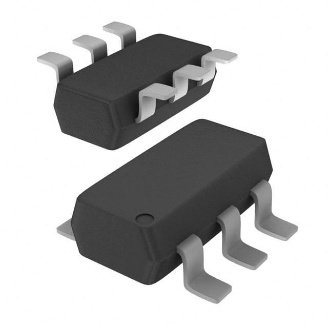
The BSL207SPH6327XTSA1 is a P-Channel enhancement mode MOSFET from Infineon Technologies, part of the OptiMOS-P small-signal transistor family. It is rated for a drain-source voltage of 20V and a continuous drain current of 6A at 25°C, with pulsed current capability up to 24A. The device features super logic level gate drive, being rated for operation at 2.5V. On-resistance is typically 29 mOhm at 4.5V (max 41 mOhm) and 43 mOhm at 2.5V (max 65 mOhm). Gate threshold voltage ranges from -0.6V (min) to -1.2V (max), with a typical value of -0.9V. The MOSFET is avalanche rated (44 mJ) and offers a reverse diode dv/dt capability of 6 kV/µs. Switching speeds are fast: turn-on delay time 9 ns typ, rise time 17 ns typ, turn-off delay 42 ns typ, fall time 53 ns typ. Input capacitance is 1007 pF, output capacitance 410 pF, and reverse transfer capacitance 332 pF at 15V. The device is housed in a P-TSOP6-6 package (SOT-23-6 thin), suitable for surface mount assembly. It is supplied in tape and reel (3000 pieces per reel). Thermal resistance junction-to-ambient is 230 K/W on a minimal footprint, improving to 62.5 K/W with a 6 cm² cooling area. The BSL207SPH6327XTSA1 is qualified to AEC-Q101, RoHS compliant, halogen free, and ESD class 1a (HBM). It is designed for applications such as battery management, load switching, DC-DC converters, and power management in portable and automotive electronics.
| Qty | Low | High |
|---|---|---|
| 1+ | $1.18 | $1.18 |
| 10+ | $0.74 | $0.74 |
| 100+ | $0.49 | $0.49 |
| 500+ | $0.38 | $0.38 |
| 1,000+ | $0.34 | $0.34 |
| 3,000+ | $0.29 | $0.29 |
| 6,000+ | $0.27 | $0.27 |
| 9,000+ | $0.26 | $0.26 |
Estimated market price range - modelled values for guidance only, not live distributor offers.
The drain-source voltage (Vds) is rated at 20V.
The continuous drain current is 6A at 25°C.
The operating junction temperature range is -55°C to 150°C.
Yes, it is RoHS3 compliant with Pb-free lead plating.
It is available in a P-TSOP6-6 package (SOT-23-6 thin).
The gate threshold voltage (Vgs(th)) is -0.6V minimum, -0.9V typical, and -1.2V maximum.
Yes, the BSL207SPH6327XTSA1 is qualified according to AEC Q101.