

| Distributor | Stock | Pricing | MOQ | PKG | Lead Time | Date Code | On Order Quantity | On Order Delivery | |
|---|---|---|---|---|---|---|---|---|---|
|
31,020 pcs
|
31020 pcs | On Request | 1 | On Request | On Request | On Request | On Request | On Request | |
|
2,893 pcs
|
2893 pcs | On Request | 1 | On Request | On Request | 21+ | On Request | On Request |
| Category | |
| Manufacturer Name | |
| AEC Qualified | |
| Automotive Grade | |
| Configuration | |
| Current | |
| Drain to Source Voltage (Vdss) | |
| FET Feature | |
| Gate Charge (Qg) (Max) @ Vgs | |
| Halogen Free | |
| Input Capacitance (Ciss) (Max) @ Vds | |
| Mounting Type | |
| Operating Temperature | |
| Power | |
| Rds On (Max) @ Id, Vgs | |
| SVHC Present | |
| Supplier Device Package | |
| Tape & Reel | |
| Technology | |
| Vgs(th) (Max) @ Id |
The BSD235CH6327XTSA1 is a complementary N and P-Channel enhancement mode MOSFET array from Infineon Technologies, part of the OptiMOS 2 and OptiMOS-P 2 small signal transistor families. It is designed for surface mount applications and is qualified according to AEC Q101, making it suitable for automotive and industrial environments.
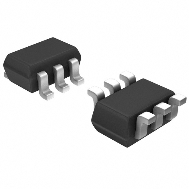
This device integrates both an N-Channel and a P-Channel MOSFET in a single SOT-363 package (PG-SOT363-6-1). The N-Channel MOSFET has a maximum continuous drain current of 0.95A at 25°C, while the P-Channel offers 0.53A. Both channels are rated for a drain-source voltage of 20V. The MOSFETs feature logic level gate drive, with gate threshold voltages of 0.7V to 1.2V for the N-Channel and -1.2V to -0.6V for the P-Channel. On-state resistance is 350 mOhm for the N-Channel at 4.5V gate drive and 1200 mOhm for the P-Channel.
The device is avalanche rated, with single pulse avalanche energy of 1.6 mJ for the N-Channel and 1.4 mJ for the P-Channel. It is 100% lead-free and halogen-free according to IEC61249-2-21. The operating temperature range is -55°C to 150°C.
Typical applications include load switching, power management, and signal switching in space-constrained designs. The compact SOT-363 package allows for high-density PCB layouts.
| Qty | Low | High |
|---|---|---|
| 1+ | $0.64 | $0.64 |
| 10+ | $0.42 | $0.42 |
| 100+ | $0.27 | $0.27 |
| 500+ | $0.18 | $0.18 |
| 1,000+ | $0.14 | $0.14 |
| 3,000+ | $0.11 | $0.11 |
Estimated market price range - modelled values for guidance only, not live distributor offers.
The drain-source breakdown voltage is 20V for both N and P-Channel MOSFETs.
It is available in a surface mount SOT-363 package (also known as 6-VSSOP, SC-88, or PG-SOT363-6-1).
The operating temperature range is -55°C to 150°C.
Yes, the device is 100% lead-free and RoHS compliant according to the datasheet.
The N-Channel MOSFET can handle 0.95A continuous drain current at 25°C, while the P-Channel handles 0.53A.
The maximum on-state resistance is 350 mOhm at Vgs=4.5V and Id=950mA.
Yes, it is qualified according to AEC Q101.