

| Distributor | Stock | Pricing | MOQ | PKG | Lead Time | Date Code | On Order Quantity | On Order Delivery | |
|---|---|---|---|---|---|---|---|---|---|
|
3,674 pcs
|
3674 pcs | On Request | 1 | On Request | On Request | 19+ | On Request | On Request | |
|
1,173 pcs
|
1173 pcs | On Request | 1 | On Request | On Request | On Request | On Request | On Request | |
|
1,000 pcs
|
1000 pcs | On Request | 1 | On Request | On Request | On Request | On Request | On Request |
| Category | |
| Manufacturer Name | |
| Gate Charge | |
| Halogen Free | |
| Mounting Type | |
| SVHC Present |
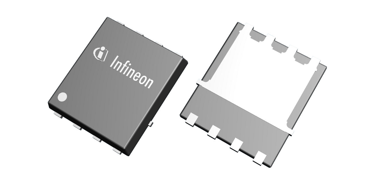
The Infineon BSC010NE2LSI is an N-channel OptiMOSTM Power MOSFET designed for high-performance buck converter applications. It features a drain-source voltage (VDS) of 25V and a maximum on-resistance (RDS(on)) of 1.05 mΩ at a gate-source voltage (VGS) of 4.5V. The device offers a continuous drain current (ID) of up to 236A at TC=25°C with VGS=10V.
This MOSFET includes a monolithic integrated Schottky-like diode and is 100% avalanche tested. It is qualified according to JEDEC standards for target applications. The BSC010NE2LSI comes in a PG-TDSON-8 package, suitable for surface mounting.
Key electrical parameters include a maximum pulsed drain current (ID,pulse) of 944A and a gate source voltage (VGS) range of ±20V. Power dissipation is rated at 96W at TC=25°C and 2.5W at TA=25°C with a thermal resistance of 50 K/W.
| Qty | Low | High |
|---|---|---|
| 1+ | $0.62 | $0.62 |
Estimated market price range - modelled values for guidance only, not live distributor offers.
The maximum drain-source voltage (VDS) for the BSC010NE2LSI is 25V.
The maximum on-resistance (RDS(on)) is 1.05 mΩ at VGS=4.5V.
The continuous drain current (ID) is rated up to 236A at TC=25°C with VGS=10V.
The BSC010NE2LSI is supplied in the PG-TDSON-8 package.
The RoHS status is RoHS3 Compliant.
The Moisture Sensitivity Level (MSL) is 1 Unlimited.