

| Distributor | Stock | Pricing | MOQ | PKG | Lead Time | Date Code | On Order Quantity | On Order Delivery | |
|---|---|---|---|---|---|---|---|---|---|
|
200 pcs
|
200 pcs | On Request | 1 | On Request | On Request | On Request | On Request | On Request |
| Category | |
| Manufacturer Name | |
| AEC Qualified | |
| Automotive Grade | |
| Current | |
| DC Current Gain (hFE) (Min) @ Ic, Vce | |
| Frequency | |
| Gain | |
| Lead Style | |
| Mounting Type | |
| Noise Figure (dB Typ @ f) | |
| Operating Temperature | |
| Power | |
| Storage Temperature | |
| Supplier Device Package | |
| Termination Style | |
| Transistor Type | |
| Voltage |
The BFU550XRR from NXP Semiconductors is an NPN wideband silicon RF transistor designed for high speed and low noise operation. It features a transition frequency (fT) of 11 GHz and a minimum noise figure of 0.7 dB at 900 MHz, making it well-suited for low-noise amplifier stages and broadband applications up to 2 GHz.
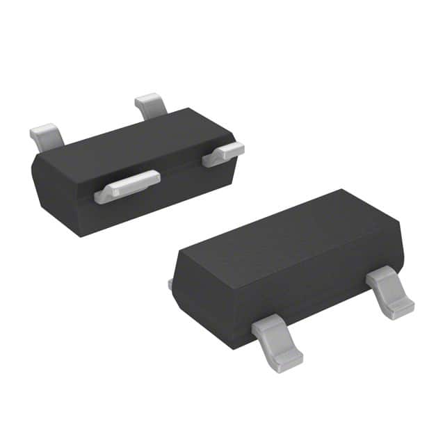
The transistor delivers a maximum stable gain of 21.5 dB at 900 MHz and an output power at 1 dB gain compression of 13.5 dBm. It is packaged in a plastic, 4-pin dual-emitter SOT143R surface-mount package with gull-wing leads. The device is AEC-Q101 qualified for automotive applications.
Key electrical ratings include a collector-emitter voltage of 12 V (open base) and a collector current of 50 mA maximum. The total power dissipation is 450 mW at a solder point temperature of 87 °C. The operating junction temperature range is -40°C to 150°C.
The maximum collector-emitter voltage is 12 V with the base open, and 24 V with the base shorted.
The typical minimum noise figure is 0.7 dB at 900 MHz with Ic = 1 mA and Vce = 8 V.
The typical transition frequency is 11 GHz at Ic = 25 mA and Vce = 8 V.
The BFU550XRR is in a surface-mount SOT-143R plastic package with 4 pins (dual emitters).
The operating junction temperature range is -40°C to 150°C.
RoHS compliance is reported as RoHS3 Compliant but is unverified based on available data.