

| Distributor | Stock | Pricing | MOQ | PKG | Lead Time | Date Code | On Order Quantity | On Order Delivery | |
|---|---|---|---|---|---|---|---|---|---|
|
8,475 pcs
|
8475 pcs | On Request | 1 | On Request | On Request | 20+ | On Request | On Request |
| Category | |
| Manufacturer Name | |
| Current | |
| DC Current Gain (hFE) (Min) @ Ic, Vce | |
| Frequency | |
| Mounting Type | |
| Noise Figure (dB Typ @ f) | |
| Operating Temperature | |
| Power | |
| Supplier Device Package | |
| Transistor Type | |
| Voltage |
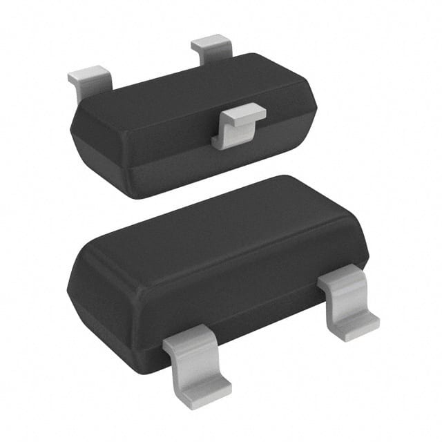
The BFT92W,115 is a silicon PNP wideband transistor designed for general purpose RF applications up to 2 GHz. Manufactured by NXP Semiconductors, it features gold metallization for excellent reliability. The transistor is housed in a plastic SOT323 (SC-70) surface-mount package with marking code W1.
Key electrical specifications include a collector-base breakdown voltage (VCBO) of 20 V, collector-emitter breakdown voltage (VCEO) of 15 V, and emitter-base breakdown voltage (VEBO) of 2 V. The maximum DC collector current is 25 mA, and total power dissipation is 300 mW at a soldering point temperature of 93 °C. The DC current gain (hFE) is a minimum of 20 at Ic = -15 mA and Vce = -10 V.
High-frequency performance is characterized by a transition frequency (fT) of 4 GHz, maximum unilateral power gain (GUM) of 17 dB at 500 MHz and 11 dB at 1 GHz, and a noise figure (F) of 2.5 dB at 500 MHz. Feedback capacitance (Cre) is 0.5 pF maximum. The transistor is suitable for wideband amplifier, oscillator, and low-noise RF front-end circuits.
The device operates over a junction temperature range up to 150 °C and can be stored from -65 °C to 150 °C. Thermal resistance from junction to soldering point is 190 K/W. The BFT92W uses the same crystal as the SOT23 version BFT92, offering a compact footprint for space-constrained designs.
The collector-base breakdown voltage (VCBO) is 20 V minimum, collector-emitter breakdown voltage (VCEO) is 15 V minimum, and emitter-base breakdown voltage (VEBO) is 2 V maximum.
The transistor is available in SC-70 (SOT-323) surface-mount package.
The junction temperature maximum is 150 °C, and storage temperature range is -65 °C to 150 °C.
The part is listed as RoHS3 Compliant, but this status is unverified.
The transition frequency (fT) is typically 4 GHz at Ic = -15 mA, Vce = -10 V, f = 500 MHz.
The DC current gain (hFE) is minimum 20 at Ic = -15 mA, Vce = -10 V.
The noise figure (F) is typically 2.5 dB at Ic = -5 mA, Vce = -10 V, f = 500 MHz.