Ready to onboard?
Are you ready to join DistyParts and
grow your business?


| Distributor | Stock | Pricing | MOQ | PKG | Lead Time | Date Code | On Order Quantity | On Order Delivery | |
|---|---|---|---|---|---|---|---|---|---|
|
141,000 pcs
|
141000 pcs | On Request | 1 | On Request | On Request | On Request | On Request | On Request |
| Category | |
| Manufacturer Name | |
| AEC Qualified | |
| AEC-Q101 Qualified | |
| Automotive Grade | |
| Collector Current - Continuous | |
| Collector Current - Peak | |
| Collector-Base Voltage (VCBO) | |
| Collector-Emitter Voltage (VCEO) | |
| DC Current Gain (Minimum @ VCE=5 V, IC=100 µA) | |
| DC Current Gain (Minimum/Maximum @ Vce=-5 V, Ic=-2 mA) | |
| Emitter-Base Voltage (VEBO) | |
| Junction Temperature (TJ) | |
| Military Grade | |
| Mounting Type | |
| Number of Pins | |
| Operating Temperature Range | |
| Power Dissipation (Ptot) | |
| Storage Temperature | |
| Storage Temperature Range | |
| Tape & Reel | |
| Thermal Resistance (Rth(j-a)) | |
| Transistor Type |
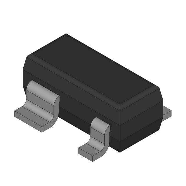
The BCV62C is a PNP general-purpose double transistor from Nexperia, housed in a compact SOT-143B surface-mount package. It integrates two matched PNP transistors, making it ideal for applications requiring consistent electrical characteristics between devices, such as current mirrors and temperature-compensated circuits.
Key electrical specifications include a maximum collector-emitter voltage (VCEO) of -30 V, a continuous collector current of -100 mA, and a peak collector current of -200 mA. The DC current gain (hFE) for the BCV62C variant is specified at 420 to 800 under test conditions of VCE = -5 V and IC = -2 mA. Each transistor also has a minimum hFE of 100 at VCE = -5 V and IC = -100 µA.
The device is AEC-Q101 qualified, suitable for automotive applications. It has a maximum power dissipation of 250 mW per device on an FR4 PCB and an operating junction temperature range of -65 to +150 °C. The SOT-143B package has 4 pins and is designed for surface mount assembly.
The BCV62C is housed in a SOT-143B surface-mount package.
The BCV62C has an operating temperature range of -65 to +150 °C.
The RoHS status is listed as compliant but is unverified.
The maximum continuous collector current is -100 mA, with a peak of -200 mA.
The DC current gain (hFE) is 420 to 800 at VCE = -5 V and IC = -2 mA.