

| Distributor | Stock | Pricing | MOQ | PKG | Lead Time | Date Code | On Order Quantity | On Order Delivery | |
|---|---|---|---|---|---|---|---|---|---|
|
6,000 pcs
|
6000 pcs | On Request | 1 | On Request | On Request | On Request | On Request | On Request |
| Category | |
| Manufacturer Name | |
| Access Time | |
| Lead Style | |
| Memory Format | |
| Memory Interface | |
| Memory Organization | |
| Memory Size | |
| Memory Type | |
| Mounting Type | |
| Operating Temperature | |
| Supplier Device Package | |
| Technology | |
| Voltage | |
| Write Cycle Time |
The AT49BV040B-JU is a 4 megabit (512K x 8) in-system reprogrammable Flash Memory manufactured by Microchip Technology. It operates with a single supply voltage ranging from 2.7V to 5.5V, offering flexibility for various applications.
This Flash Memory provides a fast read access time of 70 ns at 2.7V to 3.6V and 55 ns at 4.5V to 5.5V. It supports byte-by-byte programming with a typical time of 10 µs/byte and has a minimum of 100,000 write cycles. The device features a flexible sector architecture, including a 16K byte boot sector with programming lockout, two 8K byte parameter sectors, and eight main memory sectors.
Designed for in-system reprogrammability, the AT49BV040B-JU does not require high input voltages for programming. It utilizes standard CE, OE, and WE inputs for data access. The memory array can be erased via chip erase or sector erase command sequences. The end of program or erase cycles can be detected using DATA polling or the toggle bit feature.
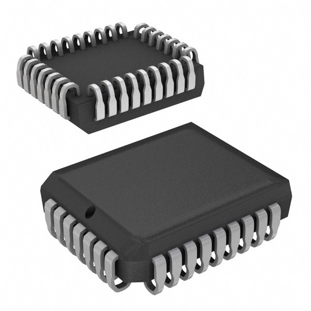
The AT49BV040B-JU is available in a 32-lead PLCC (J-Lead) package, suitable for surface mounting. It operates within an industrial temperature range of -40°C to 85°C.
| Qty | Low | High |
|---|---|---|
| 1+ | $1.28 | $1.28 |
Estimated market price range - modelled values for guidance only, not live distributor offers.
The AT49BV040B-JU operates from 2.7V to 5.5V.
The AT49BV040B-JU is available in a 32-PLCC (13.97x11.43mm) surface mount package.
The operating temperature range is -40°C to +85°C (TC).
The memory size is 4Mbit organized as 512K x 8.
The access time is 70ns at 2.7V-3.6V and 55ns at 4.5V-5.5V.
The write endurance is 100,000 cycles minimum.
The typical standby current is 25µA at 3V and 30µA at 5V.