


| Distributor | Stock | Pricing | MOQ | PKG | Lead Time | Date Code | On Order Quantity | On Order Delivery | |||||||||
|---|---|---|---|---|---|---|---|---|---|---|---|---|---|---|---|---|---|
|
2,000 pcs
|
2000 pcs | On Request | 1 | On Request | On Request | On Request | On Request | On Request | |||||||||
|
13 pcs
$92.00
|
13 pcs |
$92.00
|
1 | On Request | On Request | On Request | On Request | On Request |
| Category | |
| Manufacturer Name | |
| Clock Frequency | |
| Memory Format | |
| Memory Interface | |
| Memory Organization | |
| Memory Size | |
| Memory Type | |
| Mounting Type | |
| Operating Temperature | |
| Supplier Device Package | |
| Technology | |
| Voltage | |
| Write Cycle Time |
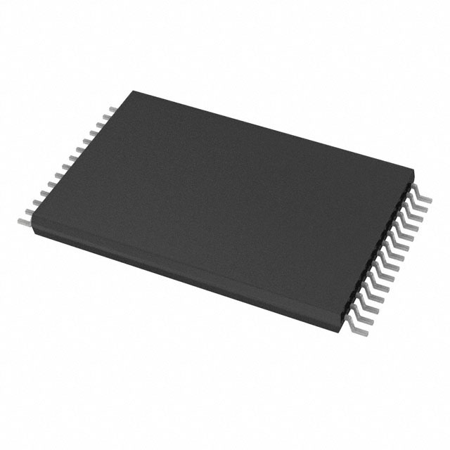
This Adesto Technologies AT45DB642D-TU is a non-volatile FLASH memory component with a capacity of 64Mbit. It features a high-speed SPI interface, capable of operating at clock frequencies up to 66 MHz. The device requires an operating voltage between 2.7V and 3.6V, making it suitable for a variety of embedded systems.
The memory is organized into pages, with a write cycle time of 6ms. The component is designed for surface mount applications and comes in a 28-TSOP package, specifically the 28-TSSOP (0.465", 11.80mm Width) variant. Its operating temperature range is -40°C to 85°C (TC).
This FLASH memory is ideal for applications requiring reliable data storage in a compact form factor. The SPI interface simplifies integration with microcontrollers, while the 64Mbit capacity provides ample storage for firmware, configuration data, or logging.
Compliance information indicates RoHS3 compliance and an MSL rating of 1. REACH status is listed as unaffected.
| Qty | Low | High |
|---|---|---|
| 1+ | $1.28 | $1.28 |
Estimated market price range - modelled values for guidance only, not live distributor offers.
The supply voltage range is 2.7V to 3.6V.
It is available in a 28-TSSOP (0.465", 11.80mm Width) surface mount package.
The operating temperature range is -40°C to 85°C (TC).
The memory density is 64 Mbit (8192 pages of 1056 bytes each).
The SPI interface supports a maximum clock frequency of 66 MHz.
It uses a SPI (Serial Peripheral Interface) memory interface.
The write cycle time is 6 ms.