

| Distributor | Stock | Pricing | MOQ | PKG | Lead Time | Date Code | On Order Quantity | On Order Delivery | |
|---|---|---|---|---|---|---|---|---|---|
|
10,000 pcs
|
10000 pcs | On Request | 1 | On Request | On Request | On Request | On Request | On Request |
| Category | |
| Manufacturer Name | |
| Clock Frequency | |
| Memory Format | |
| Memory Interface | |
| Memory Organization | |
| Memory Size | |
| Memory Type | |
| Mounting Type | |
| Operating Temperature | |
| Supplier Device Package | |
| Supplier Package | |
| Technology | |
| Voltage | |
| Write Cycle Time |
The AT25FF041A-MAHN-T from Adesto Technologies is a 4Mbit non-volatile FLASH NOR memory device. It utilizes a SPI - Quad I/O interface and operates at a clock frequency of 104 MHz. The memory organization is 2M x 2, providing ample storage for various applications.
Designed for flexibility, this memory component operates within a voltage range of 1.65V to 3.6V and has an operating temperature range of -40°C to 85°C (TC). The write cycle time is specified as 22µs for page writes and 2.6ms for buffer writes.
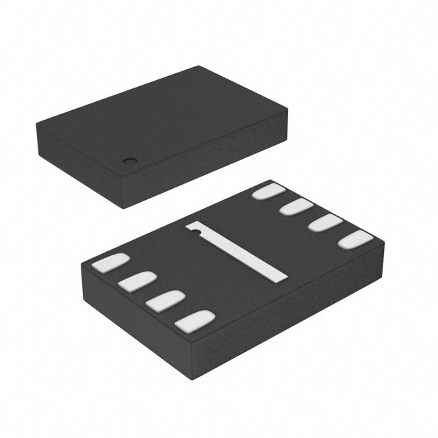
This device is supplied in an 8-UDFN (2x3) package, suitable for surface mounting. Its compact size and robust specifications make it a reliable choice for embedded systems and other applications requiring efficient data storage.
| Qty | Low | High |
|---|---|---|
| 1+ | $1.28 | $1.28 |
Estimated market price range - modelled values for guidance only, not live distributor offers.
The operating voltage is 1.65V to 3.6V.
The operating temperature range is -40°C to 85°C (TC).
It comes in an 8-UDFN Exposed Pad package (2x3 mm) for surface-mount assembly.
The memory size is 4 Mbit.
The maximum clock frequency is 104 MHz.
It supports SPI Quad I/O interface.
The write cycle time is 22 µs for page program and 2.6 ms for block erase.