

| Distributor | Stock | Pricing | MOQ | PKG | Lead Time | Date Code | On Order Quantity | On Order Delivery | |
|---|---|---|---|---|---|---|---|---|---|
|
2,782 pcs
|
2782 pcs | On Request | 1 | On Request | On Request | On Request | On Request | On Request |
| Category | |
| Manufacturer Name | |
| Clock Frequency | |
| Memory Format | |
| Memory Interface | |
| Memory Organization | |
| Memory Size | |
| Memory Type | |
| Mounting Type | |
| Operating Temperature | |
| Supplier Device Package | |
| Supplier Package | |
| Technology | |
| Voltage | |
| Write Cycle Time |
The AT25F2048N-10SU-2.7 from Microchip Technology is a 2,097,152-bit (2Mbit) serial reprogrammable Flash memory device. It is organized as 262,144 words of 8 bits each and is optimized for low-power, low-voltage industrial and commercial applications.
This device features a Serial Peripheral Interface (SPI) compatible interface, supporting SPI Modes 0 and 3 with a clock rate of up to 33 MHz. It offers byte mode and 256-byte page mode for program operations. The memory is divided into four sectors, each 64K Bytes, with 256 pages per sector. It operates within a voltage range of 2.7V to 3.6V.
Key features include sector write protection, hardware and software data protection via WP pin and Write Disable instructions, and a product identification mode. The self-timed program cycle is typically 30 µs/Byte, and the self-timed sector erase cycle is typically 1 second/Sector. The device boasts high reliability with an endurance of 10,000 typical write cycles and 20 years of data retention.
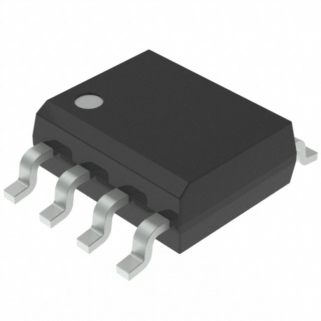
The AT25F2048N-10SU-2.7 is supplied in an 8-lead JEDEC SOIC package with a surface mount type. This compact package is suitable for space-constrained designs.
| Qty | Low | High |
|---|---|---|
| 1+ | $1.28 | $1.28 |
Estimated market price range - modelled values for guidance only, not live distributor offers.
The operating voltage for this device is between 2.7V and 3.6V.
The AT25F2048N-10SU-2.7 is available in an 8-SOIC package.
The operating temperature range is -40°C to 85°C.
The memory size is 2Mbit.
This device uses an SPI memory interface.
The maximum clock frequency supported is 33 MHz.
The typical write cycle time is 50 µs.