

| Distributor | Stock | Pricing | MOQ | PKG | Lead Time | Date Code | On Order Quantity | On Order Delivery | |
|---|---|---|---|---|---|---|---|---|---|
|
82,182 pcs
|
82182 pcs | On Request | 1 | On Request | On Request | On Request | On Request | On Request |
| Category | |
| Manufacturer Name | |
| Clock Frequency | |
| Memory Format | |
| Memory Interface | |
| Memory Organization | |
| Memory Size | |
| Memory Type | |
| Mounting Type | |
| Operating Temperature | |
| Operating Voltage | |
| Package / Case | |
| Supplier Device Package | |
| Technology | |
| Voltage | |
| Write Cycle Time |
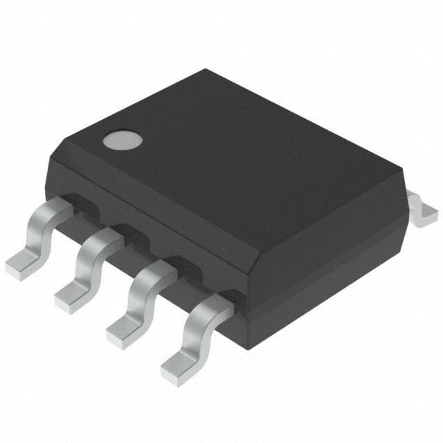
The Microchip Technology AT25F1024N-10SI-2.7 is a serial reprogrammable Flash memory device offering 1,048,576 bits of storage. It is organized as 131,072 words of 8 bits each and is optimized for low-power and low-voltage industrial and commercial applications.
This SPI-compatible memory supports SPI Modes 0 and 3 with a clock rate of up to 20 MHz. It features byte mode and 256-byte page mode for programming operations. The device operates within a voltage range of 2.7V to 3.6V and includes sector write protection capabilities.
Key features include a self-timed program cycle of 60 µs/Byte typical and a self-timed sector erase cycle of 1 second/Sector typical. The memory offers high reliability with an endurance of 10,000 write cycles typical. It is available in an 8-lead JEDEC SOIC package, suitable for surface mount applications.
The AT25F1024N-10SI-2.7 is enabled via the Chip Select (CS) pin and accessed through a 3-wire interface (SI, SO, SCK). Write protection is further enhanced by a Write Protect (WP) pin and write disable instructions for both hardware and software data protection.
| Qty | Low | High |
|---|---|---|
| 1+ | $1.28 | $1.28 |
Estimated market price range - modelled values for guidance only, not live distributor offers.
2.7V to 3.6V.
8-SOIC and 8-SAP surface mount packages.
-40°C to 85°C.
1Mbit (131072 x 8).
20 MHz.
SPI modes 0 (0,0) and 3 (1,1).
10,000 write cycles.