

| Distributor | Stock | Pricing | MOQ | PKG | Lead Time | Date Code | On Order Quantity | On Order Delivery | |
|---|---|---|---|---|---|---|---|---|---|
|
50 pcs
|
50 pcs | On Request | 1 | On Request | On Request | On Request | On Request | On Request |
| Category | |
| Manufacturer Name | |
| Configuration | |
| Drain to Source Voltage (Vdss) | |
| Input Capacitance (Ciss) (Max) @ Vds | |
| Input Impedance | |
| Mode | |
| Mounting Type | |
| Operating Temperature | |
| Power | |
| Rds On (Max) @ Id, Vgs | |
| Supplier Device Package | |
| Tape & Reel | |
| Technology | |
| Vgs(th) (Max) @ Id |
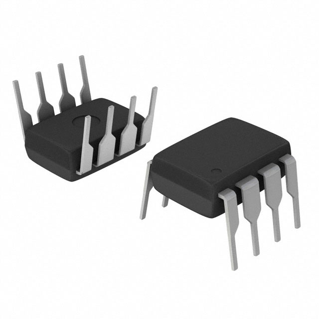
The ALD1117PAL is a monolithic dual P-channel enhancement-mode matched pair MOSFET transistor array from Advanced Linear Devices. It is designed for precision analog applications requiring high input impedance and negative current temperature coefficient. The transistor pairs are matched for minimum offset voltage and differential thermal response, making them suitable for precision analog switching and amplifying in -2V to -10V systems. Key electrical characteristics include a typical gate threshold voltage of -0.7V, low input capacitance of 3pF at 5V, and high input impedance of 10^14 ohms. The drain-source on-resistance is 1800 ohms maximum at Vgs=5V. The device operates over a temperature range of 0°C to 70°C and is housed in an 8-pin plastic DIP package (8-DIP) with through-hole mounting. The ALD1117PAL is RoHS compliant and lead-free. Typical applications include precision current mirrors, current sources, voltage choppers, differential amplifier input stages, and sample-and-hold circuits.
| Qty | Low | High |
|---|---|---|
| 1+ | $7.20 | $7.20 |
| 10+ | $5.76 | $5.76 |
| 100+ | $4.66 | $4.66 |
| 500+ | $4.14 | $4.14 |
| 1,000+ | $3.67 | $3.67 |
Estimated market price range - modelled values for guidance only, not live distributor offers.
The absolute maximum drain-source voltage is -10V.
The device is available in an 8-pin plastic DIP package (8-DIP, 0.300" lead spacing) with through-hole mounting.
The operating temperature range is 0°C to 70°C (junction temperature).
Yes, it is RoHS3 compliant and lead-free.
The typical gate threshold voltage is -0.7V at IDS = -1µA.
The maximum input capacitance is 3pF at Vds = 5V.
The typical offset voltage is 2mV (maximum 10mV) at IDS = -10µA.