

| Distributor | Stock | Pricing | MOQ | PKG | Lead Time | Date Code | On Order Quantity | On Order Delivery | |
|---|---|---|---|---|---|---|---|---|---|
|
2,500 pcs
|
2500 pcs | On Request | 1 | On Request | On Request | On Request | On Request | On Request |
| Category | |
| Manufacturer Name | |
| Current | |
| Frequency | |
| Gain | |
| Mounting Type | |
| Operating Voltage | |
| Power | |
| Storage Temperature | |
| Supplier Device Package | |
| Technology | |
| Voltage |
The AFT20S015NR1 is an N-channel enhancement-mode lateral MOSFET from NXP Semiconductors, built using LDMOS technology. It delivers 1.5 W of average output power with 17.6 dB gain and 22.0% drain efficiency at 2140 MHz under single-carrier W-CDMA conditions.
This device operates at 28 V drain voltage with a quiescent current of 132 mA. It features a drain-source breakdown voltage of 65 V and a gate-source voltage range of -6.0 to +10 V. The transistor is designed for digital predistortion error correction systems and is optimized for Doherty applications.
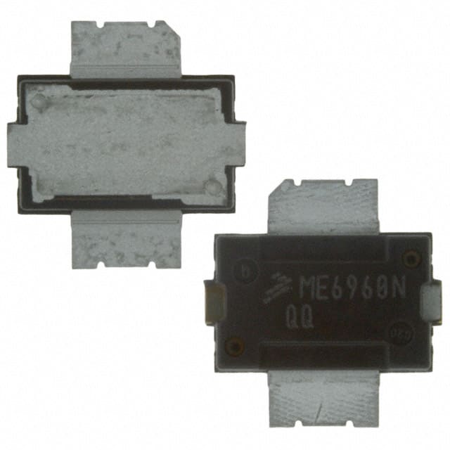
The AFT20S015NR1 is housed in a TO-270AA plastic package with a surface mount TO-270-2 supplier device package. The backside of the package serves as the source terminal for the transistor. Operating junction temperature range is -40 to +225 °C.
| Qty | Low | High |
|---|---|---|
| 1+ | $36.77 | $36.77 |
| 10+ | $29.83 | $29.83 |
| 25+ | $28.09 | $28.09 |
| 100+ | $26.18 | $26.18 |
| 250+ | $25.29 | $25.29 |
Estimated market price range - modelled values for guidance only, not live distributor offers.
The operating voltage (VDD) is 28 V DC, with a maximum rating of 32 V.
It uses a TO-270AA plastic package with a surface mount TO-270-2 supplier device package.
The operating junction temperature range is -40 to +225 °C.
The output power is 1.5 W average.
The gain is 17.6 dB at 2.17 GHz.
The device is designed for the frequency range of 1805 to 2700 MHz.