

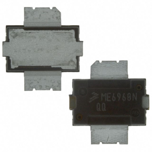
| Distributor | Stock | Pricing | MOQ | PKG | Lead Time | Date Code | On Order Quantity | On Order Delivery | |
|---|---|---|---|---|---|---|---|---|---|
|
3,421 pcs
|
3421 pcs | On Request | 1 | On Request | On Request | On Request | On Request | On Request |
| Category | |
| Manufacturer Name | |
| Current | |
| ESD Protection | |
| Frequency | |
| Gain | |
| Lead Style | |
| Mounting Type | |
| Power | |
| Storage Temperature | |
| Supplier Device Package | |
| Tape & Reel | |
| Technology | |
| Voltage |
The AFT05MS031NR1 is a high ruggedness N-channel enhancement-mode lateral MOSFET designed for mobile two-way radio applications. Operating from 136 to 520 MHz, it delivers a minimum of 31W output power (P1dB) with typical gain of 17.7 to 23.2 dB and drain efficiency up to 71.4%. The device is optimized for 13.6 V supply voltage and features integrated ESD protection and stability enhancements.
This LDMOS transistor supports broadband unmatched input and output, enabling wide frequency range utilization without external matching. It is characterized across VHF and UHF bands including 136-174 MHz, 380-450 MHz, and 450-520 MHz. The high linearity makes it suitable for TETRA, SSB, and LTE modulation schemes.
The AFT05MS031NR1 is housed in a TO-270AA surface mount package (supplier package TO-270-2) and is rated for junction temperatures up to 225°C. Thermal resistance is typically 0.67°C/W, ensuring robust thermal performance. The device is available in tape and reel packaging with 500 units per reel.
| Qty | Low | High |
|---|---|---|
| 1+ | $24.16 | $24.16 |
| 10+ | $19.34 | $19.34 |
| 25+ | $17.94 | $17.94 |
| 50+ | $17.31 | $17.31 |
| 100+ | $16.73 | $16.73 |
| 250+ | $16.27 | $16.27 |
| 500+ | $15.84 | $15.84 |
Estimated market price range - modelled values for guidance only, not live distributor offers.
The typical drain supply voltage (VDD) is 13.6 V. Maximum drain-source voltage (VDSS) is 40 V, and maximum gate-source voltage (VGS) is 12 V.
It is offered in a TO-270AA surface mount package, also designated as supplier device package TO-270-2.
The case operating temperature range is -40 to +150 °C. Storage temperature range is -65 to +150 °C. Junction temperature range is -40 to +225 °C.
It is listed as RoHS3 compliant, however this status is unverified. Please confirm with the manufacturer or authorized distributor.
Minimum P1dB output power is 31 W across 136-520 MHz (CW). At 520 MHz typical output is 33 W.
Yes, the device includes integrated ESD protection as stated in the datasheet features.
Minimum gain is 23.2 dB at 136-174 MHz, 18.3 dB at 380-450 MHz, and 17.7 dB at 450-520 MHz. Typical gain at 520 MHz is 17.7 dB.