

| Distributor | Stock | Pricing | MOQ | PKG | Lead Time | Date Code | On Order Quantity | On Order Delivery | |
|---|---|---|---|---|---|---|---|---|---|
|
4,700 pcs
|
4700 pcs | On Request | 1 | On Request | On Request | On Request | On Request | On Request |
| Category | |
| Manufacturer Name | |
| Architecture | |
| Data Interface | |
| Mounting Type | |
| Number of DACs | |
| Operating Temperature Range | |
| Output Type | |
| Power Dissipation | |
| Reference Type | |
| Resolution | |
| Supplier Device Package | |
| Supply Voltage |
The ADV7125JST330 is a triple high speed, 8-bit digital-to-analog converter (DAC) on a single monolithic chip from Analog Devices. It consists of three high speed 8-bit video DACs with complementary outputs, a standard TTL input interface, and a high impedance analog output current source. The device supports a 330 MSPS throughput rate and provides a DAC output current range of 2.0 mA to 26.5 mA.
This DAC is designed for digital video systems, high resolution color graphics, and video signal reconstruction applications. It includes an internal 1.235 V reference and operates from a single +5 V or +3.3 V supply. Typical power dissipation is 30 mW at 3 V, with a low power standby mode of 6 mW typical.
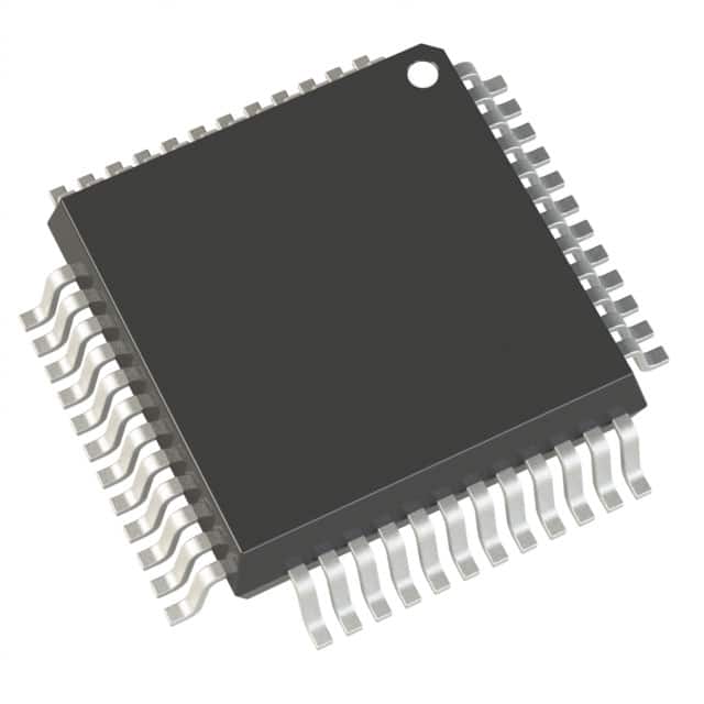
The ADV7125JST330 is housed in a 48-lead LQFP package (7x7 mm) for surface mount assembly. It is specified for the industrial temperature range of -40°C to +85°C. The device uses a parallel data interface and is built on a 5 V CMOS process.
The ADV7125JST330 has 8-bit resolution for each of its three DACs.
The maximum sampling rate is 330 MSPS at VDD = 3.3 V.
It comes in a 48-lead LQFP package (48-LQFP 7x7 mm).
The operating temperature range is -40°C to +85°C (industrial).
The device operates from a single 3.3V or 5V supply.
It provides complementary current outputs with a range of 2.0 mA to 26.5 mA.
RoHS3 Compliant per existing database entry (unverified).