

| Distributor | Stock | Pricing | MOQ | PKG | Lead Time | Date Code | On Order Quantity | On Order Delivery | |
|---|---|---|---|---|---|---|---|---|---|
|
2,010 pcs
|
2010 pcs | On Request | 1 | On Request | On Request | 24+ | On Request | On Request |
| Category | |
| Manufacturer Name | |
| Board Type | |
| Main Purpose | |
| Outputs and Type | |
| Regulator Topology | |
| Supplied Contents | |
| Tape & Reel | |
| Utilized IC | |
| Voltage |
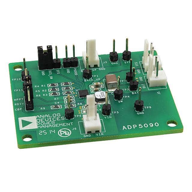
The ADP5090-1-EVALZ is an evaluation board from Analog Devices for the ADP5090, an ultralow power synchronous DC-to-DC boost regulator. The ADP5090 is housed in a compact 3 mm × 3 mm LFCSP_WQ package and integrates a power switch, synchronous rectifier, and battery management circuitry. The board is fully populated and supplied ready for use, simplifying evaluation of the regulator in low-power step-up applications.
The evaluation board operates from input voltages of 0.38 V to 3.3 V. The SYS output provides up to 3.5 V, adjustable via an external resistor divider. An internal power-good (PGOOD) indicator toggles high when the SYS pin rises to 3 V. Battery management is implemented via the SETSD pin: internal switches turn on when the storage element voltage at the BAT pin is above the externally programmed 2.4 V threshold.
This configuration makes the board suitable for evaluating the ADP5090 in ultralow power step-up applications where an efficient boost conversion is required from very low input voltages. The non-isolated output and adjustable voltage provide flexibility for various system loads.
The evaluation board is categorized under evaluation boards for DC-DC and AC-DC offline SMPS development. It includes a fully populated board assembly and documentation. The board uses the ADP5090 in a boost topology to deliver regulated output from a low-voltage source.
| Qty | Low | High |
|---|---|---|
| 1+ | $79.11 | $79.11 |
Estimated market price range - modelled values for guidance only, not live distributor offers.
The evaluation board runs from input voltages of 0.38 V to 3.3 V.
The SYS output can deliver up to 3.5 V, adjustable via an external resistor divider.
The PGOOD indicator toggles high when the SYS pin ramps up to 3 V.
Internal switches turn on when the BAT pin voltage is above 2.4 V, set via the SETSD pin.
The ADP5090 is supplied in a compact 3 mm × 3 mm LFCSP_WQ package.
The product is listed as RoHS3 compliant.
It provides one non-isolated output.