

| Distributor | Stock | Pricing | MOQ | PKG | Lead Time | Date Code | On Order Quantity | On Order Delivery | |
|---|---|---|---|---|---|---|---|---|---|
|
2,711 pcs
|
2711 pcs | On Request | 1 | On Request | On Request | 21+ | On Request | On Request | |
|
30 pcs
|
30 pcs | On Request | 1 | On Request | On Request | On Request | On Request | On Request |
| Category | |
| Manufacturer Name | |
| Current | |
| Frequency | |
| Function | |
| Mounting Type | |
| Number of Outputs | |
| Operating Temperature | |
| Output Configuration | |
| Output Type | |
| Output Voltage | |
| Supplier Device Package | |
| Synchronous Rectifier | |
| Tape & Reel | |
| Topology | |
| Voltage |
The ADP5073ACPZ-R7 from Analog Devices is a high-performance DC-to-DC inverting regulator designed to generate negative supply rails. It supports a wide input voltage range from 2.85 V to 15 V, making it suitable for various applications. The integrated 1.2 A main switch allows for an adjustable negative output voltage down to 39 V below the input voltage.
This regulator operates at a pin-selectable switching frequency of 1.2 MHz or 2.4 MHz, with the option for external synchronization between 1.0 MHz and 2.6 MHz to help manage noise in sensitive systems. It includes features such as resistor-programmable soft start, slew rate control for reduced EMI, and precision enable control. Safety features include UVLO, OCP, OVP, and TSD protection.
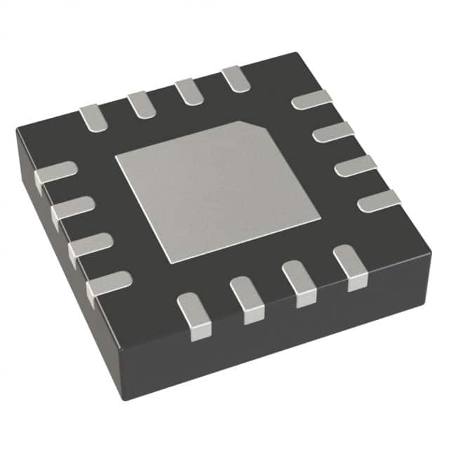
The ADP5073ACPZ-R7 is available in a 16-lead LFCSP package measuring 3 mm × 3 mm. It is rated for a junction temperature range of -40°C to +125°C. The device is supported by the ADIsimPower tool set for design assistance.
Key applications include bipolar amplifiers, ADCs, DACs, multiplexers, high-speed converters, RF power amplifier bias, and optical modules. The regulator provides a power-good output to indicate output stability.
| Qty | Low | High |
|---|---|---|
| 1+ | $0.16 | $0.16 |
Estimated market price range - modelled values for guidance only, not live distributor offers.
The input voltage range is 2.85 V to 15 V.
The output is adjustable negative, specified to VIN - 39 V.
The device supports selectable switching frequencies of 1.2 MHz and 2.4 MHz, with external synchronization from 1.0 MHz to 2.6 MHz.
The typical switch current is 1.375 A (nominal 1.2 A).
The junction temperature range is -40°C to 125°C.
The package options are 16-LFCSP (3x3) and 16-WFQFN Exposed Pad, CSP.