

| Distributor | Stock | Pricing | MOQ | PKG | Lead Time | Date Code | On Order Quantity | On Order Delivery | |
|---|---|---|---|---|---|---|---|---|---|
|
3,865 pcs
|
3865 pcs | On Request | 1 | On Request | On Request | 24+ | On Request | On Request |
| Category | |
| Manufacturer Name | |
| Data Rate | |
| ESD Protection | |
| Mounting Type | |
| Number of Drivers | |
| Number of Pins | |
| Operating Temperature | |
| Protocol | |
| Supplier Device Package | |
| Tape & Reel | |
| Type | |
| Voltage |
The ADN4662BRZ-REEL7 is a single, CMOS, low voltage differential signaling (LVDS) line receiver from Analog Devices. It is designed to convert low voltage differential input signals into a single-ended 3V TTL/CMOS logic level, supporting data rates of up to 400 Mbps (200 MHz switching rate).
The device features a flow-through pinout for simplified PCB layout and includes ±15 kV ESD protection on the input pins. It operates from a 3.3V supply voltage (3V to 3.6V range) and consumes typically 18 mW of quiescent power. The receiver offers a maximum propagation delay of 2.5 ns and conforms to the TIA/EIA-644 LVDS standard.
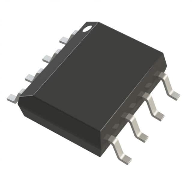
The ADN4662BRZ-REEL7 is housed in an 8-SOIC surface-mount package and is rated for an industrial temperature range of -40°C to +85°C. It is suitable for point-to-point data transmission, multidrop buses, and clock distribution networks.
The operating supply voltage range is 3 V to 3.6 V, with a typical value of 3.3 V.
The ADN4662BRZ-REEL7 is housed in an 8-SOIC (0.154", 3.90mm Width) surface-mount package.
The operating temperature range is -40°C to +85°C.
The device supports a data rate of 400 Mbps.
Yes, it features ±15 kV ESD protection on the input pins.
The maximum propagation delay is 2.5 ns.
The typical quiescent power dissipation is 18 mW.