

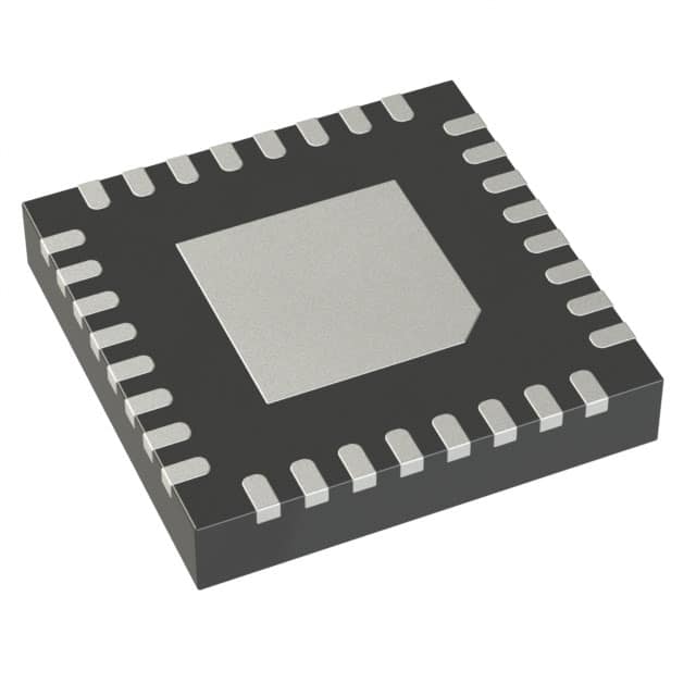
ADN2817ACPZ-RL7 Clock and data recovery IC for SONET/SDH applications, supporting continuous data rates from 10 Mbps to 2.7 Gbps. Features CML inputs and outputs, 5 mV sensitivity, and I2C control interface.
Mfr Part #:

ADN2817ACPZ-RL7

Available from 1 distributors
Mfr Name: Analog Devices / Maxim Integrated
Analog Devices / Maxim Integrated
Clock and data recovery IC for SONET/SDH applications, supporting continuous data rates from 10 Mbps to 2.7 Gbps. Features CML inputs and outputs, 5 mV sensitivity, and I2C control interface.
Total Stock: 3,000 pcs

ADN2817ACPZ-RL7 Available from 1 distributor

Authorised
Non-Authorised
Distributor Stock Pricing MOQ PKG Lead Time Date Code On Order Quantity On Order Delivery
Non-Authorised Inventory information
3,000 pcs
3000 pcs On Request 1 On Request On Request On Request On Request On Request

ADN2817ACPZ-RL7 Specifications Quick View

Most important parameters for selection – full specs in datasheet.
Category
Manufacturer Name
Control Interface
Differential
Frequency
Input
Main Purpose
Mounting Type
Number of Circuits
Operating Temperature
Output
PLL
Power Dissipation
Ratio
Sensitivity
Supplier Device Package
Voltage

ADN2817ACPZ-RL7 Description

Short technical summary and product information.

The ADN2817ACPZ-RL7 is a clock and data recovery IC from Analog Devices, part of the ADN2817/ADN2818 family. It provides quantization, signal level detection, and clock and data recovery for continuous data rates from 10 Mbps to 2.7 Gbps without requiring an external reference clock. The device exceeds all SONET jitter specifications including jitter transfer, jitter generation, and jitter tolerance.


Key specifications include a differential CML input and output, 5 mV p-p sensitivity (ADN2817 only), adjustable slice level of ±100 mV, and an I2C interface for optional features such as data rate readback, rate selectivity, and BER monitoring. The typical power dissipation is 650 mW from a 3.3V supply. The operating temperature range is -40°C to +85°C.


The ADN2817ACPZ-RL7 is housed in a compact 32-lead LFCSP package measuring 5 mm x 5 mm, suitable for surface mount assembly. It is designed for SONET/SDH, Fibre Channel, GbE, HDTV, WDM transponders, and test equipment applications.

ADN2817ACPZ-RL7 Quick Information

Product Type: Clock and Data Recovery IC
Canonical Name: ADN2817ACPZ-RL7 Clock and Data Recovery IC
Subcategory: Application Specific ClockTiming

ADN2817ACPZ-RL7 Compliance

RoHS Status: RoHS Compliant
Moisture Sensitivity Level (MSL): 1 Unlimited
REACH Status: REACH Unaffected

ADN2817ACPZ-RL7 Features

  • Supports 10 Mbps to 2.7 Gbps data rates.
  • 5 mV p-p sensitivity (ADN2817 only).
  • Adjustable slice level ±100 mV.
  • I2C interface for optional features.
  • Automatic lock without reference clock.

ADN2817ACPZ-RL7 Applications

  • Ideal for SONET OC-1 to OC-48 systems.
  • Suitable for Fibre Channel and 2x Fibre Channel.
  • Used in WDM transponder modules.
  • Applied in regenerator and repeater circuits.
  • Supports GbE and HDTV equipment.

ADN2817ACPZ-RL7 FAQs

7 frequently asked questions generated from this part’s specifications.
What is the operating voltage range of ADN2817ACPZ-RL7?

3V to 3.6V, typical 3.3V.

What is the operating temperature range?

-40°C to 85°C.

What is the package type?

32-lead LFCSP (5 mm x 5 mm).

Is the ADN2817ACPZ-RL7 RoHS compliant?

RoHS3 compliant (unverified, low confidence).

What data rates does the ADN2817ACPZ-RL7 support?

Continuous data rates from 10 Mbps to 2.7 Gbps.

Does it require an external reference clock?

No, it automatically locks to data rates without an external reference clock.

What is the input sensitivity?

5 mV p-p for ADN2817 only.

Home
Account

Categories