

| Distributor | Stock | Pricing | MOQ | PKG | Lead Time | Date Code | On Order Quantity | On Order Delivery | |
|---|---|---|---|---|---|---|---|---|---|
|
260 pcs
|
260 pcs | On Request | 1 | On Request | On Request | 22+ | On Request | On Request |
| Category | |
| Manufacturer Name | |
| Differential | |
| Frequency | |
| Input | |
| Main Purpose | |
| Mounting Type | |
| Number of Circuits | |
| Operating Temperature | |
| Output | |
| PLL | |
| Ratio | |
| Supplier Device Package | |
| Voltage |
The ADN2813ACPZ from Analog Devices is a high-performance clock and data recovery (CDR) IC designed for continuous data rates from 10 Mb/s to 1.25 Gb/s. It integrates a limiting amplifier and PLL, requiring no external reference clock for operation. The device exceeds SONET jitter requirements and is suitable for applications such as SONET OC-1/3/12, Fibre Channel, Gigabit Ethernet, and WDM transponders.
Key electrical characteristics include a single 3.3V supply operation with typical power consumption of 450 mW. The quantizer sensitivity is 3.3 mV typical, and the adjustable slice level range is ±95 mV. The loss-of-signal (LOS) detect range spans 2.3 mV to 19 mV, providing flexible signal monitoring. Input logic is CML and output logic is LVDS, both differential.
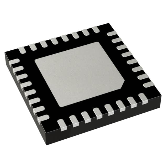
The device is housed in a compact 32-lead LFCSP package (5 mm × 5 mm) with an exposed pad for thermal management. It operates over the industrial temperature range of -40°C to +85°C. The ADN2813ACPZ is surface-mountable and lead-free, with RoHS compliance indicated.
The nominal supply voltage range is 3V to 3.6V, with a typical operating voltage of 3.3V.
The operating temperature range is -40°C to +85°C.
The device is available in a 32-lead LFCSP package (5 mm × 5 mm) with an exposed pad.
Available data indicates RoHS3 compliant status, but this is unverified and should be confirmed with official documentation.
It supports continuous data rates from 10 Mb/s to 1.25 Gb/s.
Typical power consumption is 450 mW.
The typical quantizer sensitivity is 3.3 mV.