

| Distributor | Stock | Pricing | MOQ | PKG | Lead Time | Date Code | On Order Quantity | On Order Delivery | |
|---|---|---|---|---|---|---|---|---|---|
|
3,000 pcs
|
3000 pcs | On Request | 1 | On Request | On Request | On Request | On Request | On Request | |
|
182 pcs
|
182 pcs | On Request | 1 | On Request | On Request | 07+ | On Request | On Request |
| Category | |
| Manufacturer Name | |
| Differential | |
| Frequency | |
| Input | |
| Main Purpose | |
| Mounting Type | |
| Number of Circuits | |
| Operating Temperature | |
| Output | |
| PLL | |
| Power Consumption | |
| Ratio | |
| Supplier Device Package | |
| Supplier Package | |
| Voltage |
The Analog Devices ADN2812ACPZ-RL7 is an integrated circuit designed for clock and data recovery functions. It supports a wide range of continuous data rates, from 12.3 Mb/s up to 2.7 Gb/s, automatically locking to data rates without an external reference clock.
Key electrical specifications include a typical quantizer sensitivity of 6 mV, an adjustable slice level of ±100 mV, and a loss of signal (LOS) detect range of 3 mV to 15 mV. The device operates from a single supply voltage of 3V to 3.6V, with a typical power consumption of 750 mW. It meets all SONET jitter requirements, including jitter transfer, generation, and tolerance.
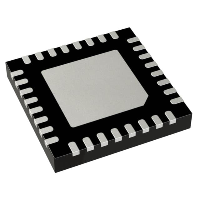
This IC is suitable for applications such as SONET OC-1/OC-3/OC-12/OC-48, Fibre Channel, GbE, and HDTV. It is housed in a compact 32-lead LFCSP package, designed for surface mounting.
The operating temperature range for the ADN2812ACPZ-RL7 is -40°C to 85°C, making it suitable for various environmental conditions.
12.3 Mb/s to 2.7 Gb/s
3.0V to 3.6V
32-LFCSP-WQ (5x5)
-40°C to +85°C
RoHS3 Compliant (unverified)
750 mW
CML