

| Distributor | Stock | Pricing | MOQ | PKG | Lead Time | Date Code | On Order Quantity | On Order Delivery | |
|---|---|---|---|---|---|---|---|---|---|
|
3 pcs
|
3 pcs | On Request | 1 | On Request | On Request | On Request | On Request | On Request |
| Category | |
| Manufacturer Name | |
| Channel Capacitance (CS(off), CD(off)) | |
| Charge Injection | |
| Crosstalk | |
| Current | |
| Mounting Type | |
| Multiplexer | |
| Number of Circuits | |
| Number of Pins | |
| On | |
| Operating Temperature | |
| Supplier Device Package | |
| Switch Circuit | |
| Switch Time (Ton, Toff) (Max) | |
| Voltage |
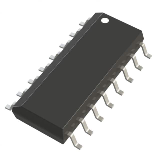
The ADG711BR is a monolithic CMOS device containing four independently selectable SPST-NC switches. It is designed for low voltage operation from 1.8V to 5.5V single supply, making it ideal for battery-powered instruments and portable electronics. The switch offers a maximum on resistance of 4.5Ω at 5V with a typical value of 2.5Ω, ensuring minimal signal loss. With a -3dB bandwidth greater than 200MHz, it is suitable for high-speed signal routing including USB 1.1, audio, and video applications. Fast switching times of 16ns (turn-on) and 10ns (turn-off) typical enable efficient signal multiplexing. The device also features low charge injection (3pC typical), low crosstalk (-90dB at 10MHz), and ultra-low power consumption (<0.01µW). It is TTL/CMOS logic compatible and qualified for automotive applications. The ADG711BR is packaged in a 16-SOIC (0.154", 3.90mm Width) surface mount package, making it easy to integrate into compact designs. Operating temperature range is -40°C to 85°C.
Maximum 4.5 Ω at 5V, typical 2.5 Ω.
1.8 V to 5.5 V single supply.
-40°C to 85°C.
16-SOIC (0.154", 3.90mm Width) surface mount.
RoHS3 Compliant (unverified, low confidence).
Turn-on time 16 ns typical, turn-off time 10 ns typical.
Greater than 200 MHz.