

| Distributor | Stock | Pricing | MOQ | PKG | Lead Time | Date Code | On Order Quantity | On Order Delivery | |
|---|---|---|---|---|---|---|---|---|---|
|
1,619 pcs
|
1619 pcs | On Request | 1 | On Request | On Request | On Request | On Request | On Request |
| Category | |
| Manufacturer Name | |
| Channel | |
| Channel Capacitance (CS(off), CD(off)) | |
| Charge Injection | |
| Current | |
| Mounting Type | |
| Multiplexer | |
| Number of Circuits | |
| On | |
| Operating Temperature | |
| Supplier Device Package | |
| Switch Time (Ton, Toff) (Max) | |
| Termination Style | |
| Voltage |
The ADG508FBRWZ is a CMOS analog multiplexer from Analog Devices that provides fault protection for both the device and signal source. It features an 8:1 multiplexer configuration with a single circuit. Key electrical specifications include a typical on resistance of 270 Ohm, maximum switch on time of 230 ns, and maximum switch off time of 130 ns. The device operates with a nominal supply voltage of ±15 V and has a typical charge injection of 15 pC. It is designed for applications requiring overvoltage protection up to -40 V to +55 V.
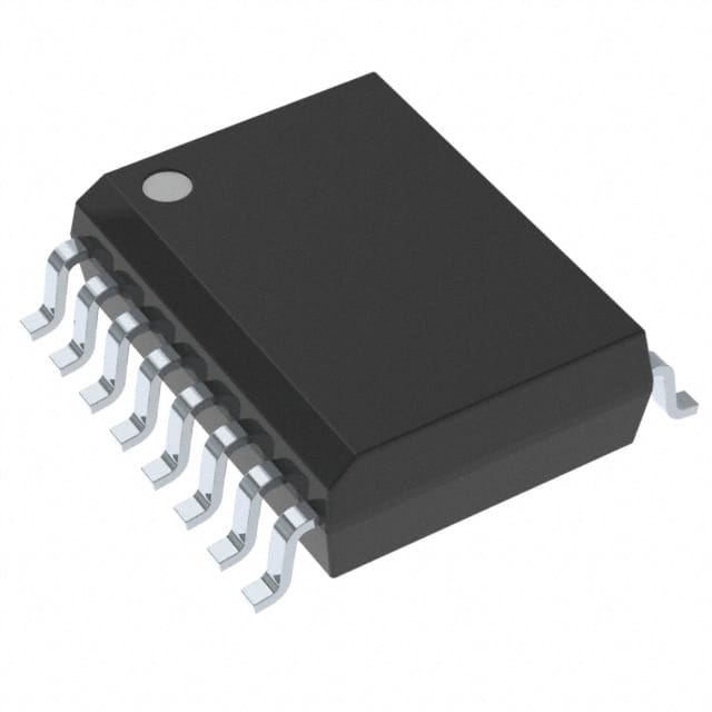
The multiplexer is housed in a 16-SOIC surface-mount package with a gull wing termination style. It operates over a temperature range of -40°C to 85°C. The device is TTL and CMOS compatible, making it suitable for a wide range of analog signal routing applications. Its break-before-make construction ensures signal integrity during channel switching.
Typical applications include existing multiplexer designs requiring fault protection, as well as new designs where multiplexer functions are needed. The low power dissipation of 3.3 mW maximum makes it suitable for power-sensitive applications.
The nominal supply voltage is ±15 V.
The device is available in a 16-SOIC surface-mount package.
-40°C to 85°C.
The RoHS status is listed as RoHS3 Compliant, but this is unverified.
Typical on resistance is 270 Ohm.
Maximum switch on time is 230 ns, maximum switch off time is 130 ns.
The multiplexer can withstand continuous overvoltage inputs from -40 V to +55 V.