

| Distributor | Stock | Pricing | MOQ | PKG | Lead Time | Date Code | On Order Quantity | On Order Delivery | |
|---|---|---|---|---|---|---|---|---|---|
|
15,000 pcs
|
15000 pcs | On Request | 1 | On Request | On Request | On Request | On Request | On Request |
| Category | |
| Manufacturer Name | |
| Channel Type | |
| Channels | |
| Mounting Type | |
| Operating Temperature | |
| Power Dissipation | |
| Supplier Device Package | |
| Supplier Package |
The ADG508FBN from Analog Devices is a CMOS analog multiplexer designed with 8 single channels. This device offers robust fault protection, safeguarding both the device and signal sources during overvoltage or power loss events. It can withstand continuous overvoltage inputs ranging from -40 V to +55 V.
Key electrical characteristics include a maximum on-resistance of 300 Ohms and fast switching times with typical values of 250 ns for both turn-on and turn-off. The multiplexer operates with low power dissipation, rated at a maximum of 3.3 mW. It is designed to prevent latch-up through trench isolation and guarantees break-before-make switching action to protect input signals.
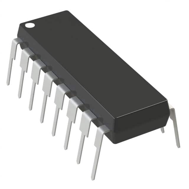
This multiplexer is housed in a 16-lead PDIP package and is designed for through-hole mounting. The ADG508FBN is suitable for applications requiring reliable signal switching and protection, particularly in environments where voltage fluctuations or potential faults may occur. Its fault protection mechanism ensures that during fault conditions, the input/output appears as an open circuit with minimal leakage current.
The maximum on-resistance for the ADG508FBN is 300 Ohms.
The ADG508FBN operates within a temperature range of -40 °C to +85 °C.
The ADG508FBN can withstand continuous overvoltage inputs from -40 V to +55 V.
The switching time for the ADG508FBN is a maximum of 250 ns for both turn-on and turn-off.
The ADG508FBN is available in a 16-PDIP package for through-hole mounting.
The ADG508FBN is RoHS3 Compliant.