

| Distributor | Stock | Pricing | MOQ | PKG | Lead Time | Date Code | On Order Quantity | On Order Delivery | |
|---|---|---|---|---|---|---|---|---|---|
|
2,860 pcs
|
2860 pcs | On Request | 1 | On Request | On Request | On Request | On Request | On Request |
| Category | |
| Manufacturer Name | |
| Configuration | |
| Lead Spacing | |
| Lead Style | |
| Mounting Type | |
| Number of Circuits | |
| Supplier Device Package |
The ADG439FBN is a CMOS analog multiplexer from Analog Devices configured as a dual 4:1 differential multiplexer. It provides fault protection for both the device and signal source in the event of an overvoltage or power loss, with a continuous overvoltage input range of -40 V to +55 V.
This multiplexer offers fast switching performance with a maximum turn-on time of 250 ns and a maximum turn-off time of 150 ns. It features break-before-make construction and is compatible with TTL and CMOS logic inputs. The device is latch-up proof and ensures that the analog output of an on channel is clamped within the power supplies if an overvoltage occurs.
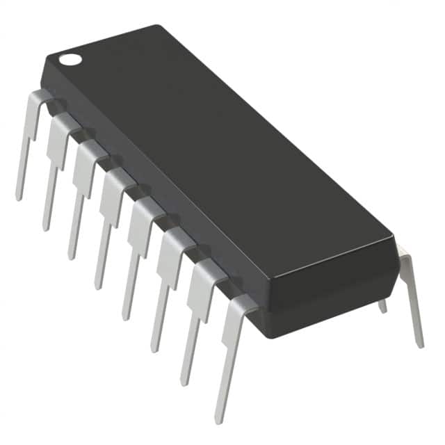
The ADG439FBN is housed in a 16-DIP (0.300", 7.62mm) package with a through-hole mounting type, supplied in a 16-PDIP supplier device package. It is suitable for data acquisition systems, industrial and process control systems, avionics test equipment, signal routing, and high reliability control systems.
The ADG439FBN is a dual 4:1 differential multiplexer.
The maximum turn-on time is 250 ns and the maximum turn-off time is 150 ns.
The fault protection voltage range is -40 V to +55 V.
The ADG439FBN is available in a 16-DIP (0.300", 7.62mm) package with a 16-PDIP supplier device package.
The mounting type is through hole.
The ADG439FBN is listed as RoHS3 compliant, though this data is unverified.