

| Distributor | Stock | Pricing | MOQ | PKG | Lead Time | Date Code | On Order Quantity | On Order Delivery | |
|---|---|---|---|---|---|---|---|---|---|
|
6 pcs
|
6 pcs | On Request | 1 | On Request | On Request | 1519 | On Request | On Request |
| Category | |
| Manufacturer Name | |
| Differential | |
| Frequency | |
| Input | |
| Mounting Type | |
| Number of Circuits | |
| Operating Temperature | |
| Output | |
| Ratio | |
| SVHC Present | |
| Supplier Device Package | |
| Supplier Package | |
| Type | |
| Voltage |
The ADCLK948BCPZ is a silicon germanium (SiGe) clock fanout buffer from Analog Devices that provides two selectable differential inputs and eight LVPECL outputs in a 2:8 configuration. It operates at frequencies up to 4.8 GHz and features 75 fs rms broadband random jitter. The device accepts CML, CMOS, LVDS, and LVPECL input logic levels and includes center-tapped 100 Ω differential on-chip input termination resistors, simplifying interface design.
The buffer is designed for low-jitter clock distribution and signal restoration in applications such as wireless and wired communications, medical and industrial imaging, ATE, and high-performance instrumentation. It runs from a 3.3 V nominal supply (2.97 V to 3.63 V) and is characterized over an operating temperature range of -40°C to +85°C. The output stages are LVPECL (positive ECL) and can be biased for LVPECL or ECL operation by connecting VCC and VEE appropriately.
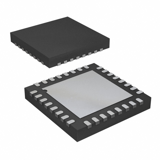
The ADCLK948BCPZ is supplied in a 32-lead LFCSP package (5 mm x 5 mm) with an exposed pad, and is intended for surface mount assembly. Its low jitter and wide input compatibility make it suitable for high-speed clock distribution in dense digital and RF systems.
The supply voltage range is 2.97V to 3.63V, with a nominal 3.3V supply.
It is available in a 32-WFQFN exposed pad CSP, also listed as 32-LFCSP (5x5) surface mount package.
The operating temperature range is -40°C to +85°C.
It is listed as RoHS3 compliant in catalog data, but this has not been independently verified.
The maximum operating frequency is 4.8 GHz.
The device provides LVPECL outputs, with eight output drivers.
CML, CMOS, LVDS, and LVPECL inputs are supported, with 100 Ω on-chip differential termination.