

| Distributor | Stock | Pricing | MOQ | PKG | Lead Time | Date Code | On Order Quantity | On Order Delivery | |
|---|---|---|---|---|---|---|---|---|---|
|
3 pcs
|
3 pcs | On Request | 1 | On Request | On Request | On Request | On Request | On Request |
| Category | |
| Manufacturer Name | |
| Data Rate | |
| Differential | |
| Frequency | |
| Input | |
| Mounting Type | |
| Number of Circuits | |
| Operating Temperature | |
| Output | |
| Propagation Delay | |
| Ratio | |
| SVHC Present | |
| Supplier Device Package | |
| Type | |
| Voltage |
The ADCLK925BCPZ-WP is an ultrafast clock/data buffer fabricated on Analog Devices' proprietary XFCB3 silicon germanium (SiGe) bipolar process. It is part of the ADCLK905/ADCLK907/ADCLK925 family and provides a single input to two differential outputs (1:2 ratio).
Key specifications include a 7.5 GHz maximum frequency and toggle rate, 10 Gbps data rate, 95 ps typical propagation delay, 60 ps typical output rise/fall time, and 60 fs random jitter. The device operates from a 2.375V to 3.63V supply voltage and over an extended industrial temperature range of -40°C to +125°C.
The inputs feature on-chip 100 Ω center-tapped termination resistors, and a VREF pin is available for biasing AC-coupled inputs. The outputs are full-swing ECL, supporting PECL (positive ECL) or NECL (negative ECL) operation depending on supply connections.
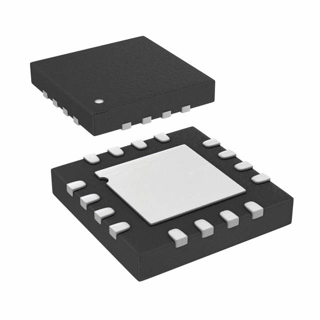
The device is offered in a 16-lead LFCSP-VQ (3x3 mm) package with an exposed pad for thermal management. It is surface mount and RoHS3 compliant (unverified).
The supply voltage range is 2.375V to 3.63V.
It comes in a 16-VFQFN Exposed Pad, CSP package, specifically a 16-LFCSP-VQ (3x3 mm).
-40°C to +125°C.
It is listed as RoHS3 Compliant, but this is unverified.
7.5 GHz.
95 ps typical.
ECL, NECL, and PECL.