

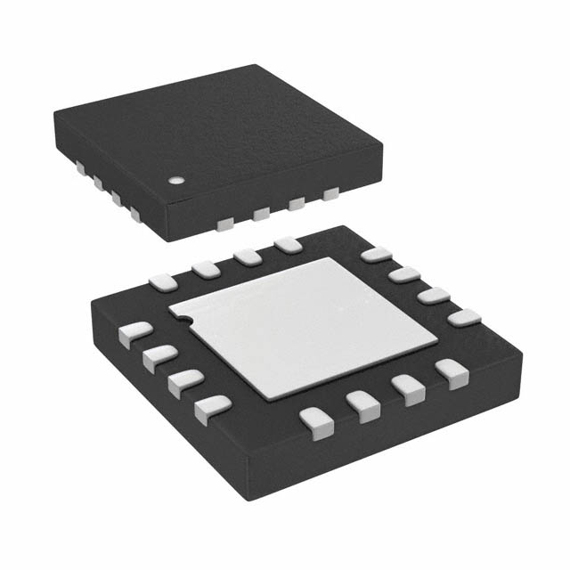
ADCLK914BCPZ-R2 The ADCLK914BCPZ-R2 is a 7.5 GHz HVDS clock/data buffer with 1:1 ratio, differential inputs and outputs, and 160 ps propagation delay. It operates from 2.97V to 3.63V and is surface mounted in a 16-LFCSP package.
Mfr Part #:

ADCLK914BCPZ-R2

Available from 2 distributors
Mfr Name: Analog Devices / Maxim Integrated
Analog Devices / Maxim Integrated
The ADCLK914BCPZ-R2 is a 7.5 GHz HVDS clock/data buffer with 1:1 ratio, differential inputs and outputs, and 160 ps propagation delay. It operates from 2.97V to 3.63V and is surface mounted in a 16-LFCSP package.
✓ Total Stock: 6,900 pcs

ADCLK914BCPZ-R2 Available from 2 distributors

✓ Authorised
✓ Non-Authorised
Distributor Stock Pricing MOQ PKG Lead Time Date Code On Order Quantity On Order Delivery
Non-Authorised Inventory information
6,898 pcs
6898 pcs On Request 1 On Request On Request On Request On Request On Request
Non-Authorised Inventory information
2 pcs
2 pcs On Request 1 On Request On Request FARNELL On Request On Request

ADCLK914BCPZ-R2 Specifications Quick View

Most important parameters for selection – full specs in datasheet.
Category
Manufacturer Name
Differential
Frequency
Input
Mounting Type
Number of Circuits
Operating Temperature
Output
Propagation Delay
Ratio
Supplier Device Package
Technology
Type
Voltage

ADCLK914BCPZ-R2 Description

Short technical summary and product information.

The ADCLK914BCPZ-R2 is an ultrafast clock/data buffer from Analog Devices Inc., fabricated on a SiGe process. It operates at a maximum frequency of 7.5 GHz with a typical propagation delay of 160 ps and output rise/fall times of 100 ps. Random jitter is only 110 fs, making it suitable for low-noise clock distribution.


The device features a single differential open-collector output with HVDS signaling, designed to drive high-speed DACs. The input includes a 100 Ω on-chip termination resistor and accepts multiple logic standards: CML, CMOS, LVDS, LVPECL, and LVTTL. A VREF pin is available for ac-coupled input biasing.


The supply voltage range is 2.97V to 3.63V, and the operating temperature range is −40°C to +125°C. The buffer is available in a 16-lead LFCSP package (3 mm × 3 mm) with exposed pad for thermal management. It is supplied in tape and reel packaging.

ADCLK914BCPZ-R2 Quick Information

Product Type: Clock Buffer/Driver, Data
Series: SiGe
Canonical Name: ADCLK914BCPZ-R2
Subcategory: Clock Buffers, Drivers

ADCLK914BCPZ-R2 Compliance

RoHS Status: RoHS Compliant
Moisture Sensitivity Level (MSL): 1 Unlimited
REACH Status: REACH Unaffected

ADCLK914BCPZ-R2 Features

  • Operates at 7.5 GHz maximum frequency.
  • 160 ps typical propagation delay.
  • 110 fs random jitter adds low noise.
  • On-chip 100 Ω input termination resistors.
  • HVDS output drives high-speed DACs.

ADCLK914BCPZ-R2 Applications

  • Clock and data signal restoration.
  • High speed converter clocking.
  • Broadband communications infrastructure.
  • High speed line receivers.
  • ATE and high performance instrumentation.

ADCLK914BCPZ-R2 FAQs

7 frequently asked questions generated from this part’s specifications.
What is the supply voltage range?

2.97V to 3.63V.

What package does the ADCLK914BCPZ-R2 come in?

16-LFCSP-VQ (3x3) or 16-VFQFN Exposed Pad, CSP.

What is the operating temperature range?

-40°C to +125°C.

Is the ADCLK914BCPZ-R2 RoHS compliant?

RoHS3 Compliant (unverified).

What is the maximum operating frequency?

7.5 GHz.

What is the propagation delay?

160 ps typical.

What input logic types are supported?

CML, CMOS, LVDS, LVPECL, LVTTL.

Home

Categories