

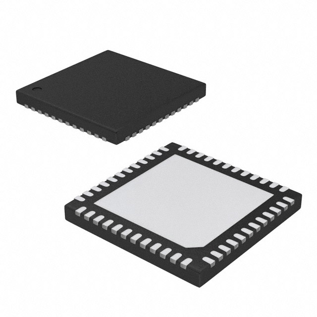
ADCLK854BCPZ-REEL7 The ADCLK854BCPZ-REEL7 is a 1.2GHz clock fanout buffer from Analog Devices. It features 2 selectable inputs, up to 12 LVDS or 24 CMOS outputs, and operates from a 1.8V supply.
Mfr Part #:

ADCLK854BCPZ-REEL7

Available from 1 distributors
Mfr Name: Analog Devices / Maxim Integrated
Analog Devices / Maxim Integrated
The ADCLK854BCPZ-REEL7 is a 1.2GHz clock fanout buffer from Analog Devices. It features 2 selectable inputs, up to 12 LVDS or 24 CMOS outputs, and operates from a 1.8V supply.
✓ Total Stock: 3,022 pcs

ADCLK854BCPZ-REEL7 Available from 1 distributor

✓ Authorised
✓ Non-Authorised
Distributor Stock Pricing MOQ PKG Lead Time Date Code On Order Quantity On Order Delivery
Non-Authorised Inventory information
3,022 pcs
3022 pcs On Request 1 On Request On Request 21+ On Request On Request

ADCLK854BCPZ-REEL7 Specifications Quick View

Most important parameters for selection – full specs in datasheet.
Category
Manufacturer Name
Control Interface
Differential
Frequency
Input
Mounting Type
Number of Circuits
Operating Temperature
Output
Power Consumption
Propagation Delay
Ratio
Supplier Device Package
Termination Style
Type
Voltage

ADCLK854BCPZ-REEL7 Description

Short technical summary and product information.

The ADCLK854 is a low jitter, low power clock fanout buffer optimized for 1.8V operation. It accepts two selectable differential inputs and supports up to 12 LVDS outputs at 1.2GHz or 24 CMOS outputs at 250MHz. Output configuration is pin programmable, allowing banks of four outputs to be set as LVDS or CMOS.


Key electrical specifications include 54 fs rms integrated jitter (12 kHz to 20 MHz), 100 fs additive broadband jitter, 2.0 ns typical propagation delay, 135 ps rise/fall time, and 70 ps output-to-output skew. Power consumption is less than 12 mW per channel at 100 MHz operation. The device also features a sleep mode for power savings.


The ADCLK854 is available in a 48-VFQFN exposed pad package (48-LFCSP-VQ 7x6.75) for surface mount assembly. It operates over the industrial temperature range of -40°C to +85°C. The device accepts a wide range of input logic levels including CML, CMOS, HSTL, LVDS, and LVPECL, making it suitable for level translation applications.

ADCLK854BCPZ-REEL7 Quick Information

Product Type: Clock Fanout Buffer
Canonical Name: ADCLK854 - 1.8V Clock Fanout Buffer with 2:12 LVDS/CMOS Outputs, 1.2GHz
Subcategory: Fanout Buffer (Distribution), Multiplexer

ADCLK854BCPZ-REEL7 Compliance

RoHS Status: RoHS Compliant
Moisture Sensitivity Level (MSL): 1 Unlimited
REACH Status: REACH Unaffected

ADCLK854BCPZ-REEL7 Features

  • Selectable LVDS or CMOS output per bank.
  • Up to 12 LVDS outputs at 1.2 GHz.
  • Up to 24 CMOS outputs at 250 MHz.
  • Low power consumption under 12 mW per channel.
  • Pin programmable control interface.

ADCLK854BCPZ-REEL7 Applications

  • Low jitter clock distribution in communications.
  • Clock and data signal restoration circuits.
  • Level translation between logic families.
  • Wireless and wired communication systems.
  • ATE and high performance instrumentation.

ADCLK854BCPZ-REEL7 FAQs

7 frequently asked questions generated from this part’s specifications.
What is the supply voltage range for the ADCLK854?

1.71V to 1.89V.

What package is the ADCLK854 available in?

48-VFQFN Exposed Pad, CSP (48-LFCSP-VQ 7x6.75).

What is the operating temperature range?

-40°C to +85°C.

Is the ADCLK854 RoHS compliant?

It is listed as RoHS3 Compliant, but this is unverified.

What is the maximum output frequency?

1.2 GHz for LVDS outputs, 250 MHz for CMOS outputs.

What logic types does the ADCLK854 support?

Inputs: CML, CMOS, HSTL, LVDS, LVPECL. Outputs: CMOS, LVDS.

What is the integrated jitter of the ADCLK854?

54 fs rms integrated jitter (12 kHz to 20 MHz).

Home

Categories