

| Distributor | Stock | Pricing | MOQ | PKG | Lead Time | Date Code | On Order Quantity | On Order Delivery | |
|---|---|---|---|---|---|---|---|---|---|
|
4,729 pcs
|
4729 pcs | On Request | 1 | On Request | On Request | On Request | On Request | On Request |
| Category | |
| Manufacturer Name | |
| Differential | |
| Frequency | |
| Input | |
| Input Type | |
| Mounting Type | |
| Number of Circuits | |
| Operating Temperature | |
| Output | |
| Power Consumption | |
| Propagation Delay | |
| Ratio | |
| SVHC Present | |
| Supplier Device Package | |
| Type | |
| Voltage |
The ADCLK854BCPZ from Analog Devices is a versatile clock fanout buffer designed for low jitter and low power applications. It supports selectable LVDS/CMOS outputs, offering configurations from 12 LVDS to 24 CMOS outputs. The device features two selectable differential inputs and accepts various logic levels including LVPECL, LVDS, HSTL, CML, and CMOS.
Key electrical specifications include a maximum input frequency of 1.2 GHz, a supply voltage range of 1.71V to 1.89V, and low power consumption of less than 12 mW per channel at 100 MHz. It boasts low integrated jitter of 54 fs rms and additive broadband jitter of 100 fs rms, making it suitable for demanding clock distribution tasks.
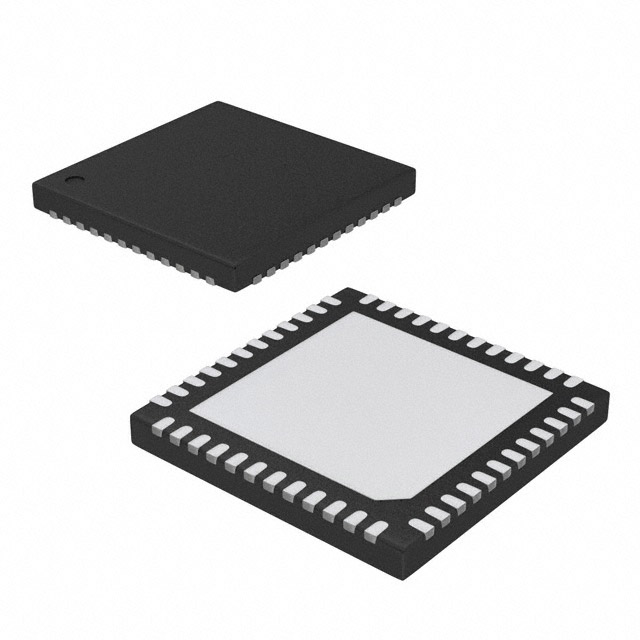
The ADCLK854BCPZ is housed in a 48-pin LFCSP package and is specified for operation over the industrial temperature range of -40°C to +85°C. Its features include a sleep mode and pin-programmable control for output configuration, enhancing its flexibility in system design.
Applications for this clock buffer include low jitter clock distribution, clock and data signal restoration, level translation, and use in wireless communications, medical imaging, and high-performance instrumentation.
The maximum input frequency for the ADCLK854BCPZ is 1.2 GHz.
The ADCLK854BCPZ operates within a supply voltage range of 1.71V to 1.89V.
The ADCLK854BCPZ supports both CMOS and LVDS output types.
The ADCLK854BCPZ is designed to operate within a temperature range of -40°C to +85°C.
The ADCLK854BCPZ is supplied in a 48-pin LFCSP-VQ (7x6.75) package.
The ADCLK854BCPZ has an integrated jitter of 54 fs rms over the 12 kHz to 20 MHz bandwidth.
The power consumption is less than 12 mW per channel during 100 MHz operation.