| Distributor | Stock | Pricing | MOQ | PKG | Lead Time | Date Code | On Order Quantity | On Order Delivery | |
|---|---|---|---|---|---|---|---|---|---|
|
9,032 pcs
|
9032 pcs | On Request | 1 | On Request | On Request | On Request | On Request | On Request | |
|
3,569 pcs
|
3569 pcs | On Request | 1 | On Request | On Request | On Request | On Request | On Request | |
|
8 pcs
|
8 pcs | On Request | 1 | On Request | On Request | On Request | On Request | 2026-04-21 02:16:43 |
| Category | |
| Manufacturer Name | |
| Differential | |
| Frequency | |
| Input | |
| Mounting Type | |
| Number of Circuits | |
| Operating Temperature | |
| Output | |
| Ratio | |
| Supplier Device Package | |
| Type | |
| Voltage |
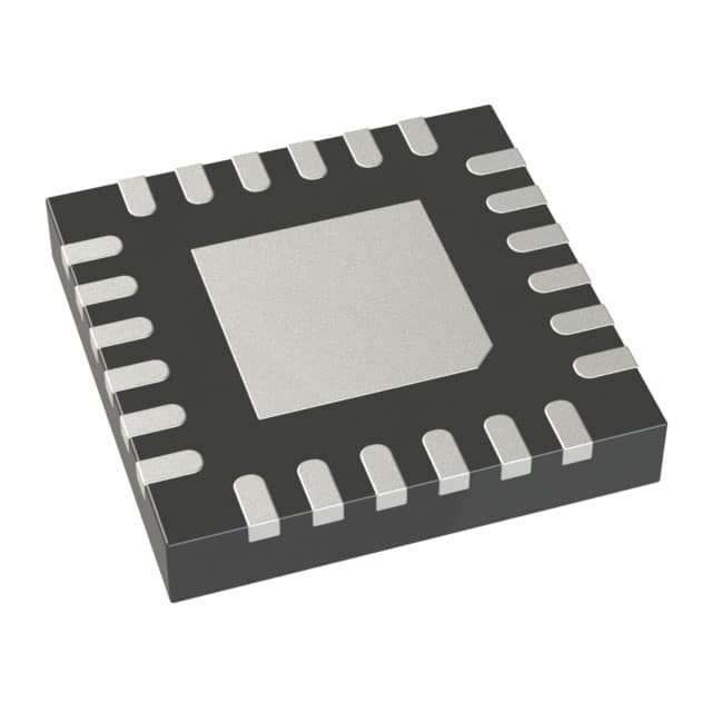
The ADCLK846BCPZ is a low power clock fanout buffer from Analog Devices, featuring selectable LVDS or CMOS outputs. It can provide up to 6 LVDS outputs at 1.2 GHz or 12 CMOS outputs at 250 MHz, or a combination. Key electrical characteristics include 54 fs integrated jitter (12 kHz to 20 MHz), 100 fs additive broadband jitter, 2.0 ns propagation delay, and 135 ps rise/fall times. Output-to-output skew is 65 ps typical. The device operates from a 1.8 V supply with less than 16 mW per channel at 100 MHz. It accepts input signals such as CML, CMOS, HSTL, LVDS, and LVPECL. The ADCLK846 is housed in a 24-LFCSP (4x4mm) package with an exposed pad for thermal management, and it is rated for surface mount assembly. Applications include low jitter clock distribution, clock and data signal restoration, and level translation in wireless and wired communications, medical imaging, and instrumentation.

1.71V to 1.89V, with a nominal supply of 1.8V.
24-LFCSP (4x4mm) surface mount package with exposed pad.
-40°C to 85°C.
RoHS3 Compliant, but this status is unverified.
1.2 GHz.
Integrated jitter (12 kHz-20 MHz) is 54 fs typical; additive broadband jitter is 100 fs typical.
Up to 6 LVDS differential outputs or up to 12 CMOS single-ended outputs, depending on configuration.