

| Distributor | Stock | Pricing | MOQ | PKG | Lead Time | Date Code | On Order Quantity | On Order Delivery | |
|---|---|---|---|---|---|---|---|---|---|
|
6 pcs
|
6 pcs | On Request | 1 | On Request | On Request | On Request | On Request | On Request |
| Category | |
| Manufacturer Name | |
| Architecture | |
| Configuration | |
| Data Interface | |
| Features | |
| Input Type | |
| Mounting Type | |
| Number of A | |
| Number of Bits | |
| Number of Inputs | |
| Operating Temperature | |
| Ratio | |
| Reference Type | |
| Sampling Rate (Per Second) | |
| Supplier Device Package | |
| Voltage |
The ADC10DV200CISQE/NOPB from Texas Instruments is a high-speed, dual-channel analog-to-digital converter (ADC) designed for demanding applications. It provides a 10-bit resolution and can achieve a maximum sample rate of 200 MSPS, making it suitable for capturing fast-changing signals.
Key electrical specifications include a typical SNR of 59.9 dBFS and an ENOB of 9.6 bits at 70 MHz. The analog input bandwidth reaches over 900 MHz, allowing for the conversion of high-frequency analog signals. The device supports both Parallel CMOS and Parallel LVDS data interfaces, offering flexibility in system integration.
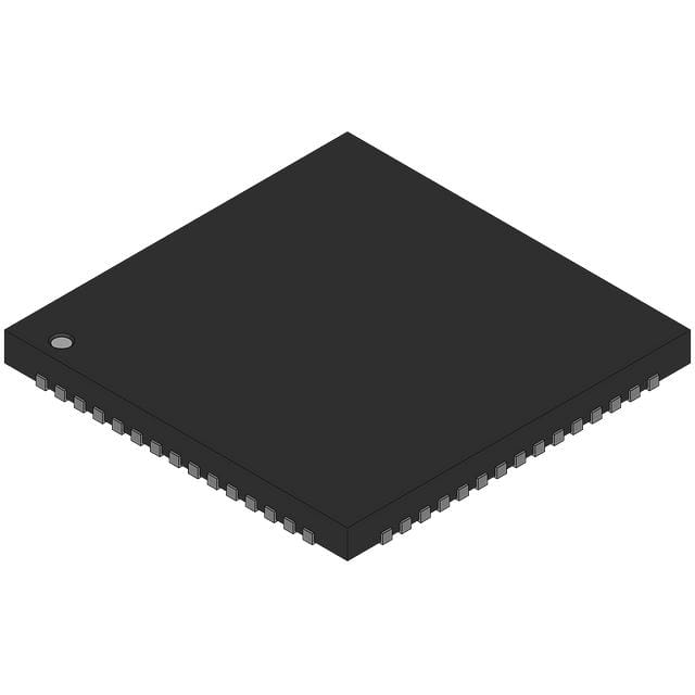
This ADC operates within a voltage range of 3V to 3.6V and features a low power consumption, typically 450mW for LVDS output at 200 MSPS and 280mW for CMOS output at 170 MSPS. It is housed in a 60-WQFN (9x9 mm) package, designed for surface mounting.
The operating temperature range is from -40°C to 85°C, ensuring reliable performance in various environmental conditions. Features like simultaneous sampling and internal or external reference options enhance its utility in complex data acquisition systems.
| Qty | Low | High |
|---|---|---|
| 1+ | $71.83 | $71.83 |
Estimated market price range - modelled values for guidance only, not live distributor offers.
The ADC10DV200CISQE/NOPB has a resolution of 10 bits.
The maximum sample rate is 200 MSPS.
The operating temperature range is -40°C to 85°C.
It is supplied in a 60-WFQFN Exposed Pad package.
It supports Parallel CMOS and Parallel LVDS data interfaces.
The analog input bandwidth is greater than 900 MHz.
The typical power consumption for LVDS output at 200 MSPS is 450mW.