

| Distributor | Stock | Pricing | MOQ | PKG | Lead Time | Date Code | On Order Quantity | On Order Delivery | |
|---|---|---|---|---|---|---|---|---|---|
|
100 pcs
|
100 pcs | On Request | 1 | On Request | On Request | On Request | On Request | 2026-06-29 21:33:16 |
| Category | |
| Manufacturer Name | |
| Architecture | |
| Configuration | |
| Data Interface | |
| Features | |
| Input Type | |
| Mounting Type | |
| Number of A | |
| Number of Bits | |
| Number of Inputs | |
| Operating Temperature | |
| Ratio | |
| Reference Type | |
| SVHC Present | |
| Sampling Rate (Per Second) | |
| Supplier Device Package | |
| Voltage |
The Texas Instruments ADC08D1520CIYB is a high-performance, low-power CMOS analog-to-digital converter. It offers 8 bits of resolution and can digitize signals at sample rates up to 3 GSPS. The device utilizes a folding and interpolating architecture, providing a typical Effective Number of Bits (ENOB) of 7.4 with a 748 MHz input signal at a 1.5 GHz sample rate.
Key features include a single +1.9V ±0.1V operation, selectable output demultiplexer modes (1:1 or 1:2), and multiple ADC synchronization capability. The data interface is LVDS - Parallel, and it operates over an industrial temperature range of -40°C to 85°C.
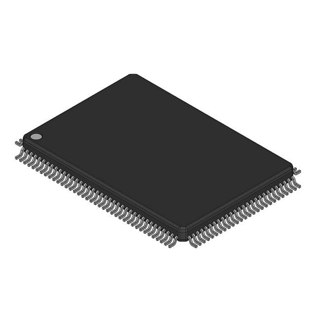
This ADC is suitable for applications such as direct RF down conversion, digital oscilloscopes, satellite set-top boxes, communications systems, and test instrumentation. It is available in a 128-HLQFP package with surface mount capability.
The ADC08D1520CIYB has an 8-bit resolution.
The maximum conversion rate is 3 GSPS.
The device operates from a single 1.9V ±0.1V supply (1.8V to 2.0V).
The operating temperature range is -40°C to 85°C.
The ADC08D1520CIYB is available in a 128-HLQFP (20x20 mm) surface-mount package.
The RoHS status is listed as RoHS3 Compliant, but this is unverified.
Typical power consumption is 1.6 W in non-demultiplexed mode at 1.0 GSPS and 2 W in 1:2 demultiplexed mode.