

| Distributor | Stock | Pricing | MOQ | PKG | Lead Time | Date Code | On Order Quantity | On Order Delivery | |
|---|---|---|---|---|---|---|---|---|---|
|
5,027 pcs
|
5027 pcs | On Request | 1 | On Request | On Request | On Request | On Request | On Request | |
|
2,443 pcs
|
2443 pcs | On Request | 1 | On Request | On Request | 1323+36 | On Request | On Request |
| Category | |
| Manufacturer Name | |
| Architecture | |
| Configuration | |
| Data Interface | |
| Input Type | |
| Mounting Type | |
| Number of A | |
| Number of Bits | |
| Number of Inputs | |
| Operating Temperature | |
| Reference Type | |
| Resolution | |
| Sampling Rate (Per Second) | |
| Supplier Device Package | |
| Voltage |
The ADC08B200CIVS is a high-speed analog-to-digital converter (ADC) from Texas Instruments with an integrated capture buffer. It offers 8-bit resolution and a maximum sampling rate of 200 MSPS, making it suitable for demanding data acquisition applications. The device features a single-ended input with a 1.6 Vpp range and a parallel CMOS data interface. Its pipeline architecture delivers typical performance of 47 dB SNR, 7.4 ENOB, 56 dB SFDR, and ±0.4 LSB DNL.
Power consumption is typically 543 mW and scales linearly with sample rate at 2 mW/Msps. A power-down mode reduces consumption to 2.15 mW. The ADC operates from a 2.7V to 3.6V supply and over a -40°C to 105°C temperature range. It is AEC-Q100 Grade 2 qualified for automotive applications.
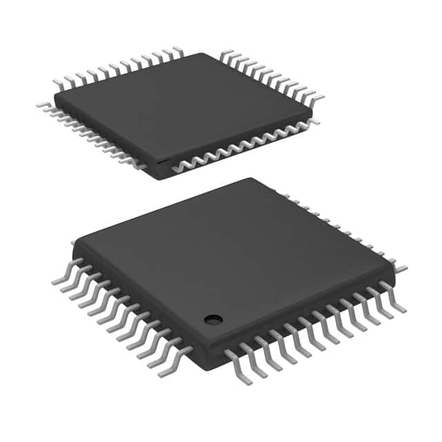
The device is housed in a 48-TQFP (7x7 mm) surface-mount package. Additional features include a selectable capture buffer size up to 1,024 bytes, an on-chip PLL for clock multiplication, and an FPGA training pattern. The reference type is external.
2.7V to 3.6V.
48-TQFP (7x7 mm).
-40°C to 105°C.
RoHS3 compliant (unverified).
200 MSPS.
8 bits.
Parallel CMOS.