

| Distributor | Stock | Pricing | MOQ | PKG | Lead Time | Date Code | On Order Quantity | On Order Delivery | |
|---|---|---|---|---|---|---|---|---|---|
|
5,750 pcs
|
5750 pcs | On Request | 1 | On Request | On Request | On Request | On Request | On Request |
| Category | |
| Manufacturer Name | |
| Input Type | |
| Mounting Type | |
| Operating Temperature | |
| Output Type | |
| Resolution | |
| Supplier Device Package | |
| Supply Voltage | |
| Type |
The AD9845BJST is a complete 12-bit, 30 MSPS CCD signal processor designed for high-performance digital still cameras and industrial/scientific imaging applications. It integrates a correlated double sampler (CDS), a 6-bit pixel gain amplifier (PxGA), a 10-bit variable gain amplifier (VGA), and a 12-bit A/D converter on a single chip.
Key electrical specifications include a supply voltage range of 2.7V to 3.6V, typical power consumption of 153 mW at 3V, and a maximum clock rate of 30 MHz. The analog-to-digital converter offers a resolution of 12 bits with no missing codes guaranteed, and typical DNL of ±0.5 LSB (maximum ±1.0 LSB). The full-scale input voltage is 2.0V, with reference top and bottom voltages of 2.0V and 1.0V respectively. Data output coding is straight binary.
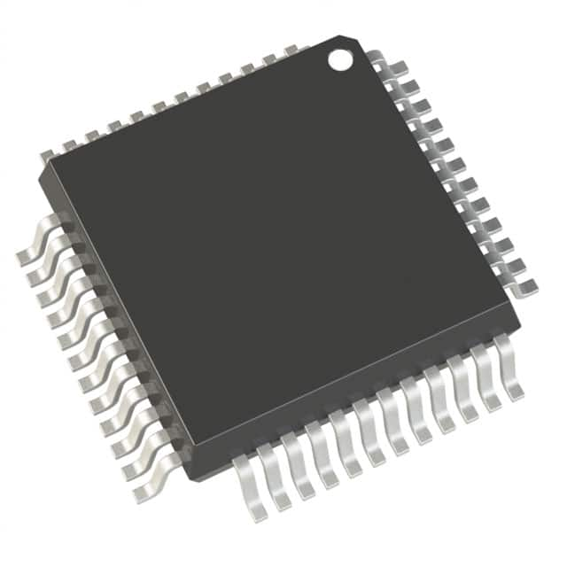
The device is housed in a 48-lead LQFP package (7x7 mm) for surface mount assembly. It operates over a temperature range of -20°C to 85°C and can be stored from -65°C to 150°C. Standby power dissipation is 5 mW typical, and total power-down mode reduces consumption to 0.5 mW typical.
Applications include high-performance digital still cameras, industrial and scientific imaging systems, and processing outputs of interlaced and progressive scan CCD arrays. The AD9845BJST is pin-compatible with earlier AD9845A designs, simplifying upgrades.
The AD9845BJST has a resolution of 12 bits.
The maximum clock rate is 30 MHz.
The supply voltage range is 2.7V to 3.6V.
The operating temperature range is -20°C to 85°C.
It comes in a 48-LQFP surface mount package (7x7 mm).
Typical power consumption is 153 mW at 3V supply.
The database lists it as RoHS3 Compliant, but this is unverified.