

| Distributor | Stock | Pricing | MOQ | PKG | Lead Time | Date Code | On Order Quantity | On Order Delivery | |
|---|---|---|---|---|---|---|---|---|---|
|
3,600 pcs
|
3600 pcs | On Request | 1 | On Request | On Request | On Request | On Request | On Request | |
|
38 pcs
|
38 pcs | On Request | 1 | On Request | On Request | 542 | On Request | On Request | |
|
15 pcs
|
15 pcs | On Request | 1 | On Request | On Request | 05+42 | On Request | On Request | |
|
5 pcs
|
5 pcs | On Request | 1 | On Request | On Request | On Request | On Request | On Request |
| Category | |
| Manufacturer Name | |
| Differential | |
| Differential Output | |
| Frequency | |
| Input | |
| Input Type | |
| Mounting Type | |
| Number of Circuits | |
| Number of Pins | |
| Operating Temperature | |
| Output | |
| Ratio | |
| Supplier Device Package | |
| Type | |
| Voltage |
The AD9515BCPZ is a high-performance clock distribution IC from Analog Devices designed for low jitter and phase noise. It features a differential clock input and two independent outputs: one LVPECL output operating up to 1.6 GHz and a second output selectable as LVDS (up to 800 MHz) or CMOS (up to 250 MHz). The device includes two programmable dividers with division ratios from 1 to 32, allowing flexible frequency synthesis. A programmable delay adjust with three selectable full-scale ranges (1.5 ns, 5 ns, and 10 ns) provides fine timing control in 16 steps per range.
Additive jitter is exceptionally low: 225 fs rms for LVPECL at 1.6 GHz, 300 fs rms for LVDS at 800 MHz, and 290 fs rms for CMOS at 250 MHz. The device operates from a 3.135V to 3.465V supply and over an industrial temperature range of -40°C to 85°C. It is housed in a space-saving 32-lead LFCSP package (5x5 mm) with exposed pad for thermal performance.
Typical applications include low jitter clock distribution for high-speed ADCs, DACs, DDSs, and mixed-signal front ends, as well as wireless transceivers, broadband infrastructure, instrumentation, and automatic test equipment. The AD9515BCPZ is configured via 4-level logic pins, simplifying setup without requiring a serial interface.
The supply voltage range is 3.135V to 3.465V.
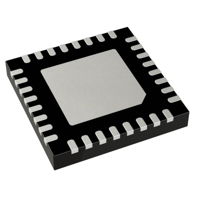
It comes in a 32-lead LFCSP (5x5 mm) package with exposed pad.
The operating temperature range is -40°C to 85°C.
The part is listed as RoHS3 compliant, but this status is unverified. Please consult the manufacturer for confirmation.
It provides one LVPECL output and one selectable LVDS or CMOS output.
The LVPECL output operates up to 1.6 GHz, LVDS up to 800 MHz, and CMOS up to 250 MHz.
Yes, it features a programmable delay adjust with three selectable full-scale ranges: 1.5 ns, 5 ns, and 10 ns, each with 16 steps of fine adjustment.