

| Distributor | Stock | Pricing | MOQ | PKG | Lead Time | Date Code | On Order Quantity | On Order Delivery | |
|---|---|---|---|---|---|---|---|---|---|
|
9,500 pcs
|
9500 pcs | On Request | 1 | On Request | On Request | On Request | On Request | On Request | |
|
2,003 pcs
|
2003 pcs | On Request | 1 | On Request | On Request | 24+ | On Request | On Request | |
|
68 pcs
|
68 pcs | On Request | 1 | On Request | On Request | On Request | On Request | On Request | |
|
8 pcs
|
8 pcs | On Request | 1 | On Request | On Request | On Request | On Request | On Request |
| Category | |
| Manufacturer Name | |
| Control Interface | |
| Differential | |
| Frequency | |
| Input | |
| Input Type | |
| Mounting Type | |
| Number of Circuits | |
| Operating Temperature | |
| Output | |
| Ratio | |
| Supplier Device Package | |
| Type | |
| Voltage |
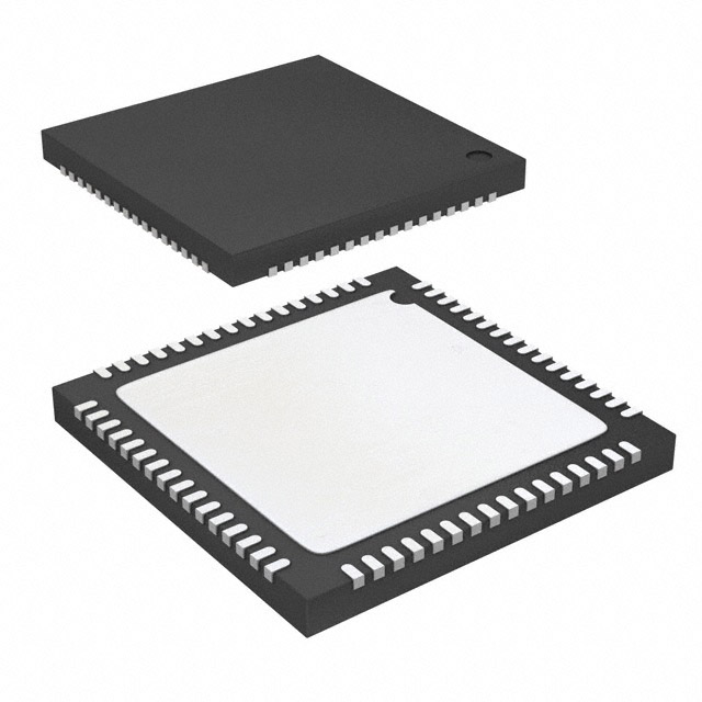
The AD9510 provides a multi-output clock distribution function along with an on-chip phase-locked loop (PLL) core. The design emphasizes low jitter and phase noise to maximize data converter performance. It operates from a 3.135V to 3.465V supply and is specified over -40°C to +85°C. The device features two differential clock inputs up to 1.6 GHz, and eight programmable dividers (1 to 32) for flexible frequency synthesis. Outputs include four 1.2 GHz LVPECL, and four independently configurable LVDS (800 MHz) or CMOS (250 MHz) outputs. Additive jitter is 225 fs rms for LVPECL and 275 fs rms for LVDS/CMOS. The device also includes a programmable charge pump, separate charge pump supply, and fine delay adjust on two outputs. It is packaged in a 64-lead LFCSP (9x9 mm) for surface mount assembly. Applications include clocking high-speed ADCs, DACs, and mixed-signal front ends, wireless transceivers, high-performance instrumentation, and broadband infrastructure.
The supply voltage range is 3.135V to 3.465V.
The operating temperature range is -40°C to +85°C.
It comes in a 64-lead LFCSP (9x9 mm) package.
RoHS3 compliant, but unverified from current data.
LVPECL up to 1.2 GHz, LVDS up to 800 MHz, and CMOS up to 250 MHz.
Eight outputs total: four LVPECL and four LVDS/CMOS configurable.
The input-to-output ratio is 2:8 (two inputs, eight outputs).