

| Distributor | Stock | Pricing | MOQ | PKG | Lead Time | Date Code | On Order Quantity | On Order Delivery | |
|---|---|---|---|---|---|---|---|---|---|
|
9 pcs
|
9 pcs | On Request | 1 | On Request | On Request | On Request | On Request | On Request |
| Category | |
| Manufacturer Name | |
| Data Interface | |
| Mounting Type | |
| Number of A | |
| Number of Bits | |
| Operating Temperature | |
| Power Dissipation | |
| Sampling Rate (Per Second) | |
| Supplier Device Package | |
| Supplier Package | |
| Supply Voltage |
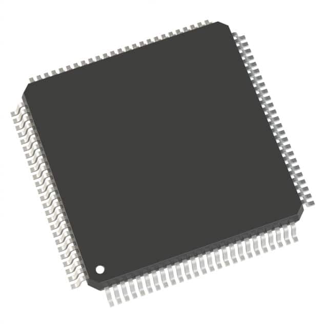
The AD9430BSV-210 is a 12-bit monolithic sampling analog-to-digital converter (ADC) from Analog Devices, optimized for high performance and low power. It supports conversion rates up to 210 MSPS and is designed for wideband carrier and broadband systems. The ADC includes an on-chip track-and-hold and reference, requiring only a 3.3 V supply and differential ENCODE clock. Key performance specifications include a signal-to-noise ratio (SNR) of 65 dB at 70 MHz input frequency, effective number of bits (ENOB) of 10.6, and spurious-free dynamic range (SFDR) of 80 dBc. The device offers excellent linearity with typical DNL of ±0.3 LSB and INL of ±0.5 LSB. The analog bandwidth is 700 MHz full-power. Power dissipation is 1.3 W typical at 210 MSPS. The digital outputs are TTL/CMOS or LVDS compatible, supporting demultiplexed CMOS outputs at 105 MSPS or LVDS at 210 MSPS. The ADC is available in a 100-lead TQFP with exposed pad (100-TQFP-EP) for surface mount assembly. It operates over the industrial temperature range of -40°C to +85°C. Typical applications include wireless and wired broadband communications, cable reverse path, test equipment, radar and satellite subsystems, and power amplifier linearization.
12 bits.
210 MSPS.
65 dB at 70 MHz input frequency.
3.3 V.
-40°C to +85°C.
100-TQFP Exposed Pad (100-TQFP-EP).
RoHS3 compliant (unverified).