

| Distributor | Stock | Pricing | MOQ | PKG | Lead Time | Date Code | On Order Quantity | On Order Delivery | |
|---|---|---|---|---|---|---|---|---|---|
|
2,750 pcs
|
2750 pcs | On Request | 1 | On Request | On Request | 24+ | On Request | On Request |
| Category | |
| Manufacturer Name | |
| Architecture | |
| Configuration | |
| Data Interface | |
| Features | |
| Input Type | |
| Mounting Type | |
| Number of A | |
| Number of Bits | |
| Number of Inputs | |
| Number of Pins | |
| Operating Temperature | |
| Power Dissipation | |
| Ratio | |
| Reference Type | |
| SVHC Present | |
| Sampling Rate (Per Second) | |
| Supplier Device Package | |
| Supplier Package | |
| Voltage |
The AD9268BCPZRL7-125 is a 16-bit, 125 MSPS dual analog-to-digital converter (ADC) from Analog Devices. It uses a pipelined architecture with two channels for simultaneous sampling, achieving a typical signal-to-noise ratio (SNR) of 78.2 dBFS at 70 MHz input frequency and 125 MSPS sampling rate. The spurious-free dynamic range (SFDR) is 88 dBc under the same conditions. Power dissipation is 750 mW typical at 125 MSPS.
The ADC accepts differential analog inputs with a flexible input voltage range of 1 V p-p to 2 V p-p and an input bandwidth of 650 MHz. It operates from a 1.8 V analog supply and supports 1.8 V CMOS or LVDS output logic. The data interface is LVDS or parallel CMOS. An on-chip duty cycle stabilizer and programmable clock divider enhance flexibility. Channel isolation is rated at 95 dB.
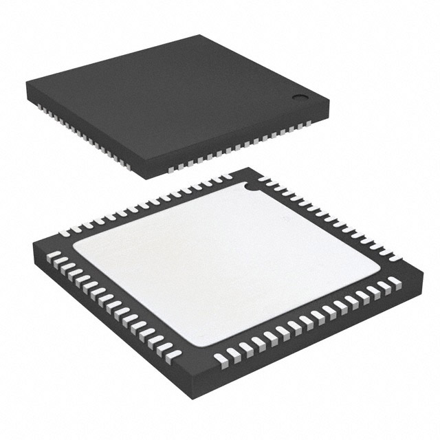
The device is housed in a 64-lead LFCSP (9x9 mm, 7.5 mm exposed pad) package for surface-mount assembly. It is rated for operation from -40°C to +85°C. Typical applications include communications receivers, software-defined radios, and ultrasound equipment.
The supply voltage range is 1.7 V to 1.9 V for the analog supply, with a typical 1.8 V operation.
The device is available in a 64-lead LFCSP (9x9 mm, 7.5 mm exposed pad) package, also described as 64-VFQFN Exposed Pad, CSP.
The operating temperature range is -40°C to +85°C.
The device is listed as RoHS3 compliant, but this status is unverified and has low confidence.
The ADC uses a pipelined architecture.
The data interface supports LVDS and parallel CMOS outputs.
Typical power dissipation is 750 mW at 125 MSPS.