

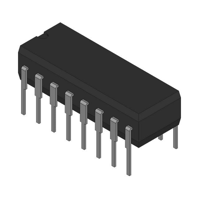
AD7522JQ The AD7522JQ is a 10-bit multiplying digital-to-analog converter from Analog Devices. It features a voltage-buffered output, single channel, and operates from 0°C to 70°C.
Mfr Part #:

AD7522JQ

Available from 1 distributors
Mfr Name: Analog Devices / Maxim Integrated
Analog Devices / Maxim Integrated
The AD7522JQ is a 10-bit multiplying digital-to-analog converter from Analog Devices. It features a voltage-buffered output, single channel, and operates from 0°C to 70°C.
Total Stock: 2,500 pcs

AD7522JQ Available from 1 distributor

Authorised
Non-Authorised
Distributor Stock Pricing MOQ PKG Lead Time Date Code On Order Quantity On Order Delivery
Non-Authorised Inventory information
2,500 pcs
2500 pcs On Request 1 On Request On Request On Request On Request On Request

AD7522JQ Specifications Quick View

Most important parameters for selection – full specs in datasheet.
Category
Manufacturer Name
Architecture
Differential Output
Mounting Type
Number of Bits
Number of D
Operating Temperature
Output Type
Supplier Device Package

AD7522JQ Description

Short technical summary and product information.

The AD7522JQ is a monolithic CMOS 10-bit multiplying D/A converter with an input buffer and holding register, allowing direct microprocessor interface. It features double-buffered inputs and supports both serial and parallel loading. The device operates with a +15V main supply and a +5V logic supply for TTL interface. Key specifications include 10-bit resolution, ±2 LSB nonlinearity (J grade), and a gain temperature coefficient of 10 ppm/FSR/°C. The AD7522JQ is packaged in a 28-pin ceramic DIP (CDIP) with through-hole mounting. It is suitable for applications requiring a multiplying DAC with buffered voltage output.

AD7522JQ Quick Information

Product Type: Digital to Analog Converter (DAC)
Canonical Name: AD7522JQ
Subcategory: Multiplying DAC

AD7522JQ Compliance

RoHS Status: RoHS Compliant
Moisture Sensitivity Level (MSL): 1 Unlimited
REACH Status: REACH Unaffected

AD7522JQ Features

  • 10-bit resolution with multiplying DAC architecture.
  • Voltage-buffered output for direct interface.
  • Double-buffered inputs for microprocessor compatibility.
  • Operates from 0°C to 70°C temperature range.
  • 28-pin ceramic DIP package.

AD7522JQ Applications

  • Ideal for microprocessor-controlled analog output systems.
  • Used in process control and instrumentation.
  • Suitable for waveform generation and signal synthesis.
  • Applicable in automatic test equipment.

AD7522JQ FAQs

7 frequently asked questions generated from this part’s specifications.
What are the supply voltage requirements?

VDD = +15V typical, VCC = +5V typical for TTL interface.

What is the package type?

28-pin ceramic DIP (CDIP) with 0.600 inch width.

What is the operating temperature range?

0°C to 70°C.

Is the AD7522JQ RoHS compliant?

RoHS3 compliant according to database, but unverified.

What is the resolution of the AD7522JQ?

10 bits.

What is the architecture of the AD7522JQ?

Multiplying DAC.

What is the nonlinearity specification?

±2 LSB maximum at 25°C (J grade).

Home
Account

Categories