

| Distributor | Stock | Pricing | MOQ | PKG | Lead Time | Date Code | On Order Quantity | On Order Delivery | |
|---|---|---|---|---|---|---|---|---|---|
|
3,566 pcs
|
3566 pcs | On Request | 1 | On Request | On Request | On Request | On Request | On Request |
| Category | |
| Manufacturer Name | |
| Data Interface | |
| Lead Style | |
| Mounting Type | |
| Output Type | |
| Reference Type | |
| Resolution | |
| Settling Time | |
| Supplier Device Package |
The AD7248JP is a complete 12-bit voltage output digital-to-analog converter (DAC) from Analog Devices, part of the AD7248A family. It integrates a precision output amplifier and a 5 V buried Zener reference on a single CMOS chip, requiring no external trims for full specified performance.
This DAC features an 8-bit-wide data bus with double-buffered interface logic, allowing data to be loaded in two write operations. It offers a typical settling time of 5 µs and guarantees ±0.5 LSB integral and differential nonlinearity. The device operates from analog and digital supplies of 12 V to 15 V and consumes typically 65 mW in single-supply mode.
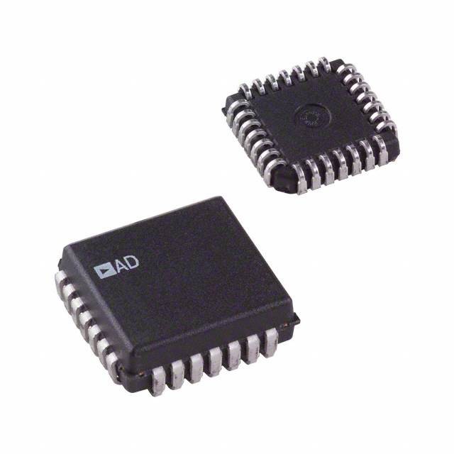
The AD7248JP is designed for industrial temperature range operation from -40°C to +85°C. It is housed in a 28-pin PLCC (J-Lead) package for surface mount assembly. The part is suitable for applications requiring a compact, high-performance DAC with internal reference and minimal external components.
The AD7248JP has a resolution of 12 bits.
The typical settling time is 5 µs.
The operating temperature range is -40°C to +85°C.
The AD7248JP is available in a 28-PLCC (11.51x11.51 mm) surface mount package.
Yes, it includes an internal 5 V buried Zener reference.
The analog and digital supply voltage range is 12 V to 15 V.
The maximum INL and DNL is ±0.5 LSB.